The 68th annual IEEE International Conference on Electronic Devices in San Francisco. iEDM is the premier conference for state-of-the-art semiconductor device technology. At this year's conference, organizations including Intel, TSMC, Samsung, IBM, Micron, Shinsei, Sunrise, Applied Materials and countless others, research institutions such as IMEC and CEA-Leti, and then several universities showcased cutting-edge semiconductor technologies. Cutting edge here means not only the most advanced logic processes, but also memory, analog, packaging and many other areas. It is important to stay tuned to this conference because it showcases technologies that will lead to changes in the business of devices, foundries, fabless, equipment, and packaging.
This paper is part of a short series on the many advances, developments and research discussed at IEDM, which will cover advanced logic technologies and advanced packaging. This paper will cover CFET - the next evolution of GAA transistors, Sequential Stacking, LFETs, Barrierless Tungsten Metal Stack, Samsung Hybrid Bonding Logic 4um and HBM, ASE FoCoS, TSMC 3nm FinFlex and self-aligning contacts, Intel EMIB 3 and Foveros Direct, Qualcomm Samsung 5nm DTCO & Yield, IBM Vertical Transfer FET (VTFET) and RU interconnect.
TSMC FinFlex
At IEDM 2022, TSMC talked about N3B and N3E. In the paper on N3E, TSMC introduced FinFlex, which is part of a huge design technology co-optimization (DTCO) into the N3 node family. Typically, with fin depopulation, the number of NMOS and PMOS fins in a standard cell is reduced. This allows for lower cell heights and thus higher densities. With more advanced nodes, each fin can also carry more drive current, allowing for a reduced number of fins with minimal impact on performance.
However, as cell (cell) height decreases, interconnect becomes a more limiting factor. With 1-fin cells, there is almost no interconnect space and interconnects will almost certainly be the only bottleneck. For FinFlex, a 2-1 fin setup is used, where 1 fin cells are stacked on top of 2 fin cells. This helps alleviate the interconnect bottleneck and efficiently produces cells with a height of 1.5 fins. With N3E, TSMC offers three libraries, a 2-1 cell library for high density, a 2-2 cell library for balanced power and performance, and a 3-2 cell library for high performance.
According to TSMC, the 2-1 cell library consumes 30% less power for the same performance, delivers 11% more performance for the same power, and reduces area by 36% relative to the 2-fin library on its N5 node. 2-2 cell library consumes 22% less power for iso-performance, 23% more performance for iso-power, and reduces area by 28%. The 3-2 unit library offers 12% lower power iso-performance, 32% higher performance iso-power, and 15% less area.
.jpg)
The N3E also offers six threshold voltage options, eLVT, uLVT, uL-LVT, LVT, L-LVT, and SVT, each with different tradeoffs in power and performance and allowing designers to more precisely tune their power performance characteristics.
When comparing 2-1 and 3-2 cells, TSMC shows a 9% higher performance for 3-2 cells. Unless the designer absolutely needs this performance, the performance gain is minimal. This strengthens the case for denser, more energy-efficient libraries. However, this ignores interconnect density limitations. FinFlex enables designers to achieve the highest density using lower density cells, such as 2-2 and 3-2 cells, to maximize interconnect wiring and performance.
The metal stack of N3E is slightly more relaxed than N3B but still very dense. metal 0 has a pitch of 23nm, an 18% reduction over N5. metal 0 also offers double width for lower resistance and higher performance.
TSMC has incorporated an innovative liner in the copper interconnect to reduce the resistance of the lower metal layers. We believe this liner is ruthenium, which Intel also uses as a liner in its 10nm nodes. contact resistance is reduced by 20-30% and through-hole resistance is reduced by 60%. TSMC also mentioned that the three key layers that required double patterning using EUV on N3B have been replaced by single patterning using EUV on N3E. This reduces complexity, cost and cycle time.
The N3E will be the most advanced node in production when it enters high volume production later this year. TSMC will continue to dominate the logic frontier. Innovations like FinFlex show that TSMC is forging ahead.
TSMC 3nm Self-Aligned Contacts
(Self-Aligned Contacts N3B)
Since TSMC's transition to FinFETs on N16, fin profiles have been critical to improving performance and reducing power consumption. While TSMC was able to reduce the gate length from 16-23nm on N7 to 12-14nm on N3B, TSMC also mentioned that gate length scaling has reached its limit. Even with fin optimization, TSMC was unable to reduce this further. This further emphasizes the importance of design technology co-optimization (DTCO) for further scaling into the future. In addition, it was mentioned that FinFET transistor architectures have reached their limits and must move to nanosheet transistor architectures. With N3B, TSMC has also implemented Self-Aligned Contacts (SAC: Self-Aligned Contacts). This is very interesting because Intel has been implementing SAC since 22nm. meanwhile, TSMC's first node to adopt this technology was N3B. in addition, they removed SAC from N3E. The landing area of the contacts has been significantly reduced due to the proportional difference between the contact polysilicon pitch and gate length. Tighter alignment tolerances and overlap problems caused by multiple masks have exacerbated this situation.
SAC allows the contacts to fall even on top of the gate without shorting out the transistor. While this increases process complexity and therefore cost, it improves yields. Unfortunately, it also affects performance as the gate-SD contact capacitance increases significantly.
TSMC's solution on N3B allows leakage at the gate contact junction to remain constant, even over wider gate lengths and process variations (where the contact and gate are aligned with different parts of the gate). sAC also reduces contact resistance by 45% and variation by 50%. This allows for better electrostatics and performance, as well as higher manufacturing yields.
As the gap between gate and contact continues to decrease and due to FinFET construction, TSMC faces the problem of increasing capacitance at the gate contact junction. While thicker spacers can alleviate this problem, this creates other issues, such as higher contact resistance. Inevitably, TSMC wanted to lower the dielectric constant and use a low k material. While k=1 for air is promising, TSMC's TCAD simulations show that it has less impact than switching to a dielectric with k<4.0. This raises the maximum voltage by more than 200mV and reduces the capacitance at the junction by 2.5%. These are just a few of the minor details that may be overlooked when optimizing a new process technology.
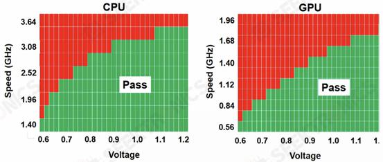
TSMC also showed a shmoo plot of the test chip on their N3B node, which showed the CPU core reaching 3.5 GHz at 1.2 V and the GPU core reaching 1.7 GHz at 1.2 V. They also showed a shmoo plot of the SRAM in the chip, which was still functioning at as low as 0.5 V.
Qualcomm and Samsung DTCO
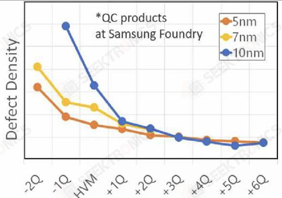
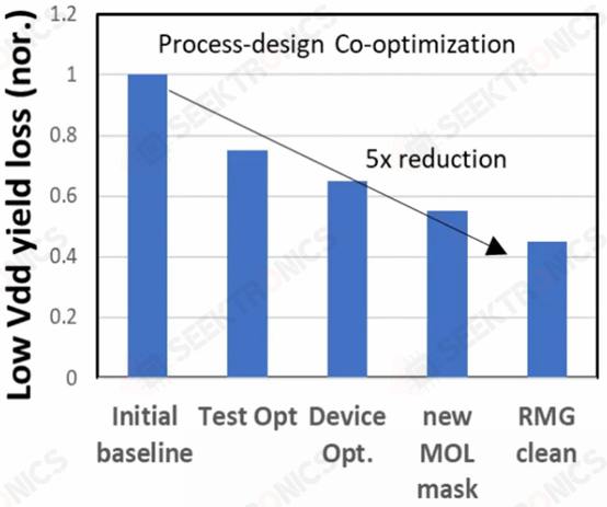
At IEDM, Qualcomm and Samsung also talked about DTCO on the Samsung 5LPE node with Snapdragon 888. Qualcomm said that the smallest fin pitch (FP), CGP, metal pitch and SRAM bit cells were used to achieve a 25 percent reduction over 7LPP. These changes can be seen in 5LPE's Ultra High-Density library. However, these shrinkages are accompanied by increased process risk. From inception to initial production, Samsung reduced defects by 60% and further reduced them to 2% of the baseline with high-volume manufacturing. 5LPE also experienced excellent yield improvements, faster than 10LPE and 7LPP. Part of the reason for this is also that 5LPE is an incremental improvement over 7LPP.
Qualcomm and Samsung also worked with DTCO to significantly improve yields, reducing yield loss by a factor of 2.5 for low-voltage operation, a key use case for mobile SoCs. They also reduced the number of defective devices by a factor of 9, which is significant.
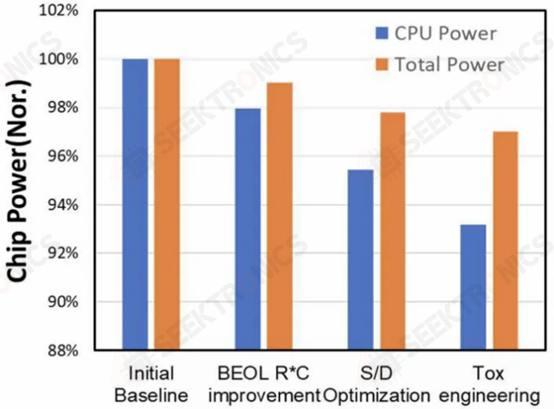
Qualcomm and Samsung also reduced CPU power by 7% and total power consumption by 3% through sustained DTCO. As process node scaling becomes slower, DTCO will become increasingly important to achieve the desired characteristics of the chip.
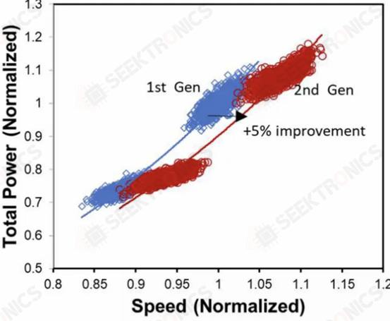
Samsung also compared their first generation node, 5LPE, to their second generation node, 5LPP. They show that it achieves 5% higher performance at the same power. 5LPP is also used in Snapdragon 8 Gen 1, sold under the 4LPX name.
Advanced Logic Technology: Transistor Architecture
After Gate All-Around FETs (GAAFETs) and Forksheets, the industry may move to Complementary FETs (CFETs), where NMOS nanosheets are stacked on top of PMOS nanosheets, and vice versa. This is a difficult process because the formation of P-type and N-type requires very high temperature epitaxial growth. Wherever you make the 2nd one, you are exposing the 1st one to high temperatures, which can destroy it. TSMC, Intel, and IMEC have all studied this. To fabricate CFETs, there are two methods, sequential and monolithic.
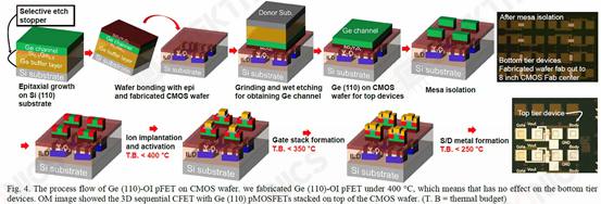
I. Heterogeneous 3D Sequential CFET composed by direct wafer bonding with Ge Nanosheet p-FET A Sequential CFET fabrication method has been proposed by Korea Advanced Institute of Science and Technology (KAIST). kaist solved the temperature problem by using a sequential stacking method in which they perform high temperature epitaxial growth and then grow them individually by In this method, they perform high temperature epitaxial growth and then combine them individually by inter-wafer bonding. The bottom pFET is composed of Ge, while the top nFET is composed of Si.

This new approach allows for a more preferred orientation of the Ge lattice with higher electron mobility. This is a way to mitigate the drive current problem of pFETs, which has been particularly severe in recent frontier nodes. The process of adding top nFETs has been tested to not affect the electrical characteristics of the bottom pFETs.
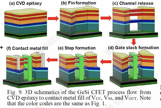
II. Monolithic 3D self-aligned GeSi channel and common-gate complementary FETs grown by CVD epitaxy National Taiwan University demonstrated their work on monolithic CFET IEs without wafer bonding. This can be achieved by low temperature (400C) epitaxial growth, which will prevent the destruction of previously fabricated structures. They fabricated SiGe channels with 75% Ge and 25% Si and used P/N junctions to isolate the two halves of the CFET. With their approach, they were able to successfully stack two pFET channels on top of 1 nFET channel.
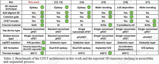
While stacked pFETs on top of stacked nFETs have been demonstrated before, this is the first time a pFET with a P/N junction has been demonstrated, and the process appears to have little effect on the formation of the source and drain. They claim that this is easier to implement than previous methods.
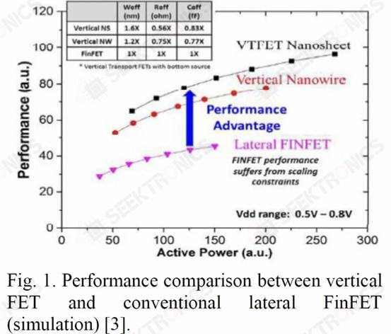
III.IBM Vertical Transfer Nanosheets
Unlike other companies in the industry, IBM sought a different approach with a different transistor architecture, one that uses vertical nanosheets. This architecture is called Vertical Transfer FET (VTFET).
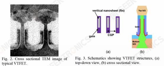
One advantage of this approach is that it allows the CGP to be miniaturized much more. Scaling the CGP beyond 40nm using conventional transistor architectures will prove extremely difficult and may involve excessive trade-offs in terms of resistance and capacitance.
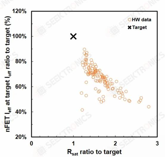
This time they are showing a VTFET with a CGP of 40nm, using dual diffusion interrupts. They also said that a zero diffusion disruption design is possible. Although IBM was able to fabricate such VTFETs, they found that the capacitance was 20% higher than analog, the drive current was lower than expected, and the optimal chip was 90% of the target.
IBM demonstrated impressive performance improvements over vertical nanowires by moving to this architecture.
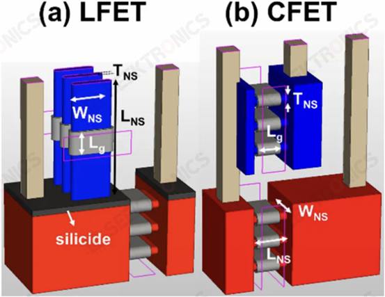
IV. Heterogeneous L-shaped field-effect transistors (LFETs) for the E technology node
Several Taiwanese universities demonstrated a new transistor architecture, the LFET. in some ways, it is a combination of IBM's VTFET and CFET. pFET is placed vertically on top of a horizontally placed nFET. the "L" in LFET does not stand for anything, it is just the shape of the structure. LFETs offer fewer density improvements, but they are easier to implement and easier to tune. The contact with the gate can also be formed more easily.
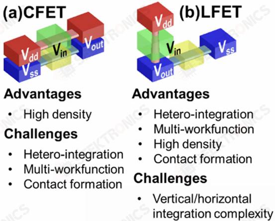
These devices are simulated using 3 PMOS and 3 NMOS nanosheets. the voltage drop of the LFETs is slightly higher. However, they also have lower power consumption and resistance.
Advanced Logic Technology: Transistor Architecture
The scaling of metal stacks is critical in every chip design, as it is often the limiting factor. However, recent technological advances have hindered the scaling of metal stacks. When current passes through a metal interconnect, it generates heat and causes a flow of metal atoms, called electromigration. Over time, this flow can lead to voids and mounds, resulting in increased device resistance and eventually failure. The problem is exacerbated by the shrinking size of copper interconnects as current density increases, leading to greater heat generation and electromigration, as well as more power loss in the interconnect compared to transistor switching. To address this problem, tantalum nitride barriers were introduced, but as the interconnects continued to shrink, the smaller the barrier size, the larger the percentage of the lower metal layer, which prevented scaling efforts. Cobalt is used in Intel's 10nm and Intel 7 nodes for the bottom metal stack, although this has been returned in Intel 4. Ruthenium is also used in their 10nm and 7nm nodes and is increasingly becoming the material everyone wants to adopt over.
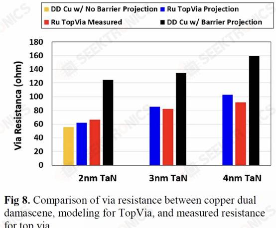
I. IBM Subtractive Ru Interconnect Implemented by a new patterning solution for EUV double patterning and TopVia with embedded air gap integration for post-Cu interconnect scaling IBM Research and Samsung demonstrated their new interconnect using ruthenium (Ru) instead of copper. Much like cobalt, Ru does not require a potential barrier and can be scaled to smaller widths without gaining astronomical resistance and capacitance.
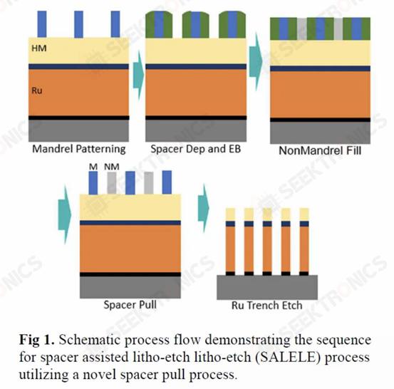
Although Ru interconnects can be fabricated using a dual-mosaic process similar to copper, they used subtractive patterning in this new study. This required the use of a spacer-assisted LELE with EUV (SALELE). This allowed them to form interconnects with a metal pitch of 18 nm, which is 22% less than the MMP on TSMC's N3E.
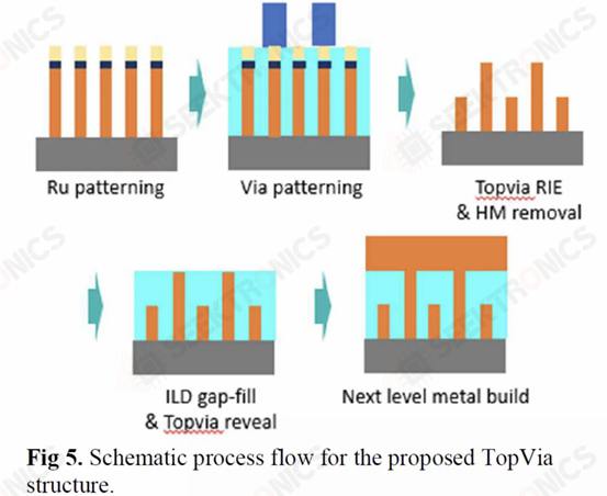
They also have a high aspect ratio of 4:1, reducing resistance by 20% at the cost of increased capacitance. Because SALELE builds vias between the metal layers on top of the interconnect, it is much easier to fill the space between the wires with air, which is the best dielectric available at ak=1. This is a significant change from low-k dielectrics with k<2.7, which can reduce capacitance by more than 30%.
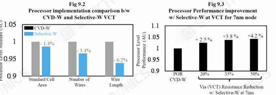
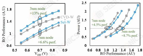
Applied Materials Tungsten MOL Local Interconnect Innovation: Materials, Processes, and Systems Synergistically Optimized for 3nm Node and Beyond Applied Materials also demonstrated their new interconnect using tungsten (W). Currently, tungsten is deposited by chemical vapor deposition (CVD) and has a barrier layer made of titanium nitride. Lam Research is leading the market share in tungsten deposition due to 3D NAND, but Tokyo Electron and Applied Materials are also operating. This new research demonstrates selectivity without a liner W. When using tungsten, the current liner is typically TiN.
If this technology is successful, it could be adopted in all advanced logic nodes, which would be a huge boon for Applied Materials.
Very similar to Ru, this is likely a candidate to allow future interconnect expansion. With this new innovation, they were able to reduce through-hole and chain resistance by 40%.
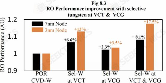
They also showed that the process can result in up to 13% better performance at the same voltage, 8.7% better performance at the same power, and 1.4% less standard cell area. Small innovations like this compound together to keep the wheels of semiconductor scaling turning.
This has tremendous potential for signal-side interconnects in future devices with backside powered networks!
Advanced Logic Technology: Static Random Access Memory (SRAM)
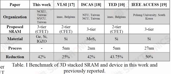
I. Integrated design and process for 3-D heterogeneous 6T SRAM with double-layer transfer Ge/2Si CFETs and IGZO transfer gates to reduce cell size by 42% As TSMC's N3E process shows, SRAM scaling is becoming exceptionally difficult. While continued gains will continue to be difficult to achieve, SRAM has some final tricks up its sleeve. The shift to GAAFET and CFET should enable significant SRAM shrinkage, 30-40% each. Several universities in Taiwan have demonstrated an SRAM bit cell design with CFET that uses only the area of 2 transistors to build a 6-transistor SRAM bit cell. They achieved this by sequential stacking.
With this, they were able to reduce the area by 42%. According to their research, the new bitcell design consumes 100 times less power at idle!
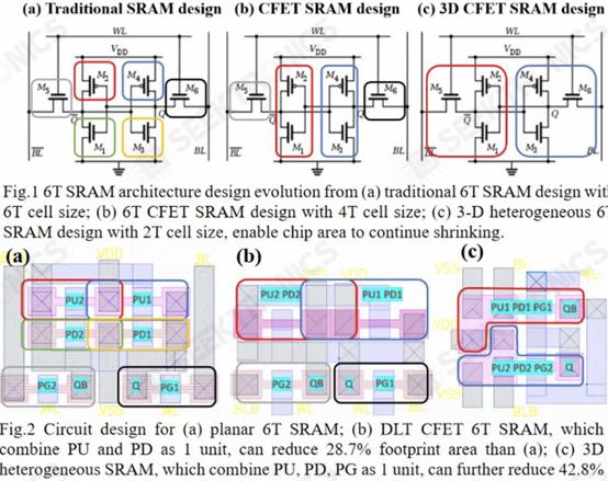
This is very interesting compared to other potential new SRAM designs moving into the 3D space, including those from IMEC. This research is critical given that TSMC's N3E does not have SRAM miniaturization.
Advanced Packaging
TSMC, Intel and Samsung provided updates on their advanced packaging technologies at IEDM. Advanced packaging will only become more important as the cost of leading edge nodes increases further.
I. TSMC Heterogeneous and Small Chip Integration using Organic Intermediary Layer (CoWoS-R) TSMC has made some minor updates to CoWoS-R. While this is mostly a restatement of existing information, TSMC says they can package in 2μm/2μm or 1μm/1μm L/S. They also showed it being used to link HBM3 to small chips.
<p class="M


-20x20-20x20.png)

