Now whenever you open the SoC original PCB Layout Guide, will mention the high-speed signal alignment of the corner angle problem, will say that high-speed signals do not take a right angle alignment, to a 45-degree angle alignment, and will say to take the arc will be better than 45-degree corners.
People began to struggle with the corner angle of the PCB alignment, that is, the last decade or two. In the early 1990s, Intel, the dominant player in the PC industry, led the customization of PCI bus technology.
(At that time, the old wu thanked Intel for releasing the PCI interface, it is with the PCI bus interface bandwidth enhancement, including the later AGP bus interface, to give birth to graphics cards like 3DFX VOODOO Voodoo, the old wu at that time also experienced the first Tomb Raider Lara Croft style, and the cool Need for Speed 2, the classic Thor's Hammer, etc. In retrospect, it is the market demand for 3D games and other multimedia applications, to promote the development of PC technology, including (Later, the Internet and the popularity of smartphones.)
It seems that starting with the PCI interface, we are entering an era of "high-speed" system design.
After the 1990s, it is a group of players like old Wu desired 3D performance, so that the corresponding electronic design and chip manufacturing technology can be developed in accordance with Moore's Law, due to the continuous improvement of the IC process, the IC transistor switching speed is also getting faster and faster, the clock frequency of various buses is also getting faster and faster, signal integrity issues are also constantly attracting research and attention. For example, now people demand 4K HD home video and audio video, HDMI2.0 transmission standard rate has reached 18Gbps!
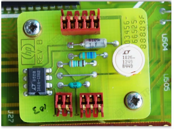
Before I was born, PCB cable pulling fungus should still be relatively simple for students, the line pulls through, jerk smooth, neat and beautiful can be, do not have to pay attention to a variety of signal integrity issues. For example, the following figure shows the HP classic HP3456A six-and-a-half-bit multimeter circuit board, a large number of 90 ° angle alignments.
HP3456A no teardrop, almost intentionally right-angle (some places would have been an oblique angle to go through, it is biased to go several consecutive right angles), the vast majority of places without laying copper.
In the upper right corner, the line width has become smaller than the right angle?
Right angles, bridging, copper laying, simulation can not really lay copper?
Right angle, 45 degree diagonal, any angle diagonal, square pads, round pads, but no teardrop.
PCB can not be sharp-edged alignment
PCB can not be sharp angle alignment, the answer is no, regardless of the sharp angle alignment will not have a negative impact on high-speed signal transmission lines, from the PCB DFM side alone, should be avoided in the case of sharp angle alignment. Because the intersection of PCB conductors to form an acute angle, will cause a problem called acid traps. In the pcb manufacturing process, in the pcb line etching process, at the "acid traps" will cause excessive corrosion of the pcb line, bringing the pcb line false break problem. Although, we can use CAM 350 for DFF Audit to automatically detect the potential problem of "acid traps" to avoid processing bottlenecks in the PCB when manufacturing, if the PCB factory processors detect the presence of acid traps, they will simply paste a piece of copper into the gap.
So we should try to avoid acid trap from the source in the layout.
How to avoid sharp angles when pulling wires, causing acid trap DFM problems? Modern EDA design software (such as Cadence Allegro, Altium Designer, etc.) are equipped with perfect Layout alignment options, we are in the layout alignment, flexible use of these auxiliary options, we can greatly avoid the layout of the "acid trap" phenomenon.
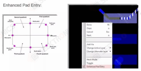
Solder pad out of the line angle settings, to avoid the formation of sharp angles between the wire and pad angle of the nip.
Using Cadence Allegro's Enhanced Pad Entry feature, we can avoid the "acid traps" DFM problem by avoiding pinch angles between traces and pads during layout as much as possible.
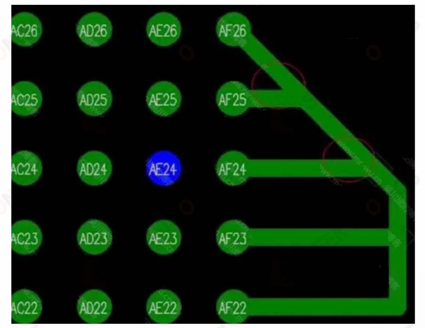
Avoid crossing two wires to form an acute angle pinch.
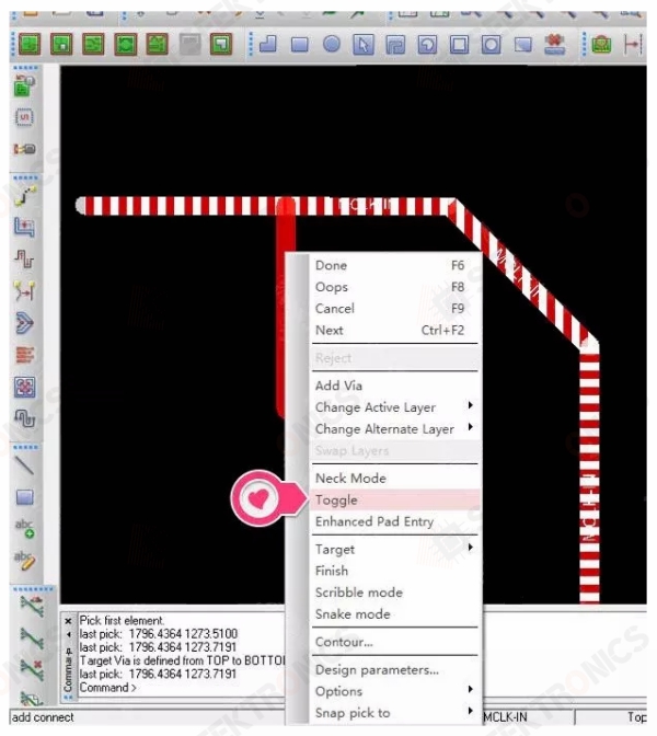
By flexibly toggling the "toggle" option when laying out Cadence Allegro wires, you can avoid the formation of sharp angle pinches when the wires are pulled out of the T-branch and avoid causing "acid traps" DFM problems.
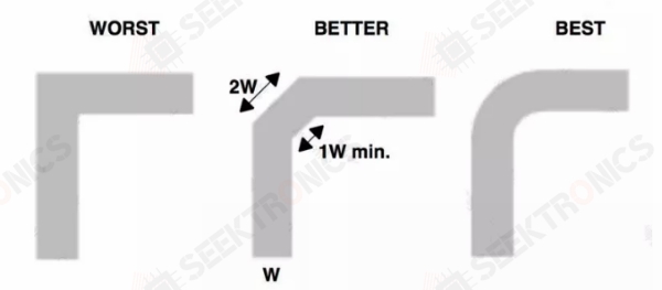
PCB layout can not be 90 ° alignment
High-frequency high-speed signal transmission lines should avoid 90 ° corner alignment, is a variety of PCB Design Guide is strongly requested, because high-frequency high-speed signal transmission lines need to maintain the same characteristic impedance, and the use of 90 ° corner alignment, in the transmission line corner, will change the line width, 90 ° corner line width is about 1.414 times the normal line width, due to the change in line width, it will cause the reflection of the signal, at the same time, the corner of the additional parasitic capacitance will also be on the The additional parasitic capacitance at the corners also has a delay effect on the signal transmission.
Of course, when the signal propagates along the uniform interconnect line, there is no reflection and no distortion of the transmitted signal. If there is a 90° corner on the uniform interconnect line, it will cause a change in the PCB transmission line width at the corner, which is calculated according to the relevant electromagnetic theory, and this will definitely bring about the reflection effect of the signal.
So, 90 ° angle on the high-speed signal transmission line will have a negative impact, theoretically certain, but the impact is not fatal? 90 ° angle for high-speed digital signals and high-frequency microwave signal transmission lines is not the same impact?
According to the paper "right angle corners on printed circuit board traces, time and frequency domain analysis" and Howard Johnson's article "Who's Afraid of the Big Bad Bend?" and Eric Bogatin's book "Signal Integrity and Power Integrity Analysis (Second Edition)" Chapter 8, we can draw the following conclusions.
For high-speed digital signals, 90° corners on high-speed signal transmission lines will cause a certain impact, for our current high-density high-speed pcb, the general alignment width of 4-5mil, a 90° corner of the capacitance of about 10fF, measured by the capacitance caused by the accumulation of time delay is about 0.25ps, so the 5mil wire width of the 90° corner does not have a high impact on the current High-speed digital signals (100-spec rising edge time) do not have a significant impact.
For high-frequency signal transmission lines, in order to avoid the skin effect (Skin effect) caused by signal damage, usually use a wider signal transmission line, such as 50Ω impedance, 100mil line width, the 90 ° corner of the line width of about 141mil, the parasitic capacitance caused by the signal delay of about 25ps, at this time, 90 ° corner will cause very serious impact The 90° corner will have a very serious impact.
At the same time, microwave transmission lines always want to minimize signal loss, 90 ° corner impedance discontinuity and outside the parasitic capacitance will cause high-frequency signal phase and amplitude errors, input and output mismatch, as well as the possible existence of parasitic coupling, which in turn leads to the deterioration of circuit performance, affecting the PCB circuit signal transmission characteristics.
The impact of a single 90° corner on the signal quality of a high-speed digital transmission line, relative to the deviation of the wire height from the reference plane, the deviation of the uniformity of the wire width and spacing during the etching of the wire itself, the variation of the sheet dielectric constant on the frequency signal, and even the impact of the over-hole parasitic parameters are much greater than the problems caused by the 90° corner.
But today's high-speed digital circuits always avoid the need to wrap around equal lengths, dozens and dozens of corners superimposed, the cumulative impact of these 90° corners superimposed on the signal rise delay will become non-negligible. High-speed signals are always transmitted along the path of least impedance, with 90 ° corner around the equal length, the final actual signal transmission path will be slightly shorter than the original.
The current HDMI 2.0 standard, the transmission bandwidth rate has reached 18Gbps, 90° corner alignment will no longer meet the requirements, and now in the 21st century, the current EDA software even those free to use, the 45 ° alignment has been well supported.
At the same time, the 90 ° corner alignment, in terms of engineering aesthetics, is not quite in line with the aesthetics of people. So, for the layout now, regardless of whether you go to the high-frequency/high-speed signal lines, we should try to avoid the 90 ° corner for the alignment, unless there are special requirements.
For high-current alignment, sometimes we will lay copper skin to replace the way wiring, in the corner of the copper laying, also need to replace the 90 ° corner with two 45 ° corner, so that not only beautiful but also does not exist EMI potential problems.
Alignment at 45°
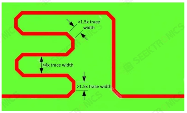
Except for RF signals and other signals with special requirements, the alignment on our PCB should preferably be at 45°. It is important to note that the length of the wire at the corners should be at least 1.5 times the width of the wire when the 45° angle is wound in equal lengths, and the spacing between the wires should be at least 4 times the width of the wire when wound in equal lengths.
Since high-speed signal lines always follow the path with the lowest impedance, if the spacing between equal-wound lines is too close, the high-speed signal will take a shortcut due to the parasitic capacitance between the lines, and the equal length will be inaccurate. The winding rules of modern EDA software are easy to set the relevant winding rules.
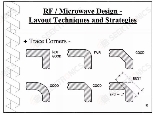
To arc arc alignment
If the technical specifications do not clearly require the arc alignment, or rf microwave transmission line, old wu personally feel that there is no need to go arc line, because the layout of high-speed high-density pcb, a large number of arc line later repair line is very troublesome, and a large number of arc alignment is also relatively expensive space. For similar USB3.1 or HDMI2.0 such high-speed differential signals, the old wu think you can still go under the arc line to pretend.
Of course, for RF microwave signal transmission line, or priority to take the circular arc line, or even to go "using 45 ° outside the diagonal cut" line alignment.
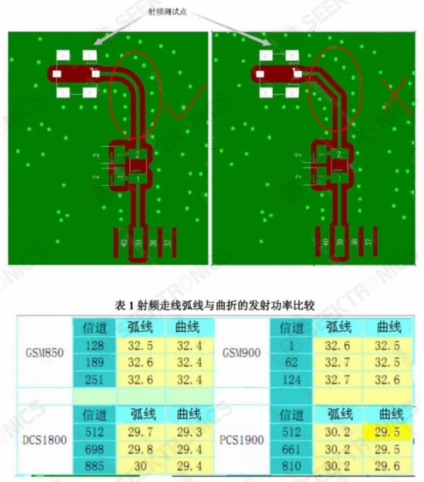
The figure below shows the RF signal transmission line arc alignment and 45 degree angle alignment power comparison results, it can be proved that the high frequency signal arc alignment is indeed due to 45 ° angle alignment.
Alignment at any angle
With the development of 4G/5G wireless communication technology and the continuous upgrading of electronic products, the current PCB data interface transmission rate has been as high as 10Gbps or 25Gbps or more, and the signal transmission rate is constantly moving in the direction of high-speed development. With the development of high-speed signal transmission, high-frequency, PCB impedance control and signal integrity put forward higher requirements.
For digital signals transmitted on PCB boards, many dielectric materials used in the electronics industry, including FR4, have been considered uniform at low speed and low frequency transmission.
However, when the electronic signal rate on the system bus reaches the Gbps level, this uniformity assumption no longer holds, when the local variation in the relative dielectric constant of the dielectric layer caused by the gap between the glass fiber bundles interwoven in the epoxy resin substrate will not be negligible, and the local disturbance in the dielectric constant will make the delay and characteristic impedance of the line spatially dependent, thus affecting the transmission of high-speed signals.
The test data based on the FR4 test substrate shows that the measured effective permittivity of the transmission line fluctuates greatly due to the difference in the relative position of the microstrip line and the glass fiber bundle, and the difference between the maximum and minimum values can reach △εr=0.4. Although these spatial perturbations appear to be small, it can seriously affect the differential transmission line with a data speed of 5-10Gbps.
In some high-speed design projects, we can use zig-zag routing techniques to mitigate the effects of fiberglass effects on high-speed signals in order to cope with them.
Cadence Allegro PCB Editor 16.6-2015 and later versions support zig-zag routing mode.
Select "Route -> Unsupported Prototype -> Fiber Weave Effect" in the Cadence Allegro PCB Editor 16.6-2015 menu to turn on the zig-zag routing feature.


-20x20-20x20.png)

