Chip area size
Chip size is determined by the chip designer and even the entire chip design team to communicate together, the chip is definitely not how big you want to design how big, there are many aspects of the cost and benefits involved, in general, under the same conditions of the architecture, the larger the chip design specifications, the higher the performance, but subject to various conditions, the chip can never be expanded without limit.
For example, a PC chip and cell phone chip design standards are different, the size of an Intel CPU in more than 100 square millimeters is very normal, and high-end i7 and to strong processor to more than 200 square millimeters is also commonplace, because the PC is larger, better heat dissipation space, the chip specifications can be made larger to improve performance.
For cell phone chips, a Snapdragon or Kirin processor can only be controlled within a few dozen square millimeters of area, because the space inside the phone inch by inch, can not withstand too large chips.
If the CPU chip occupies one-third of the phone area, the rest of the battery, all kinds of sensors and cameras will be greatly affected, the large chip brings heat and power consumption will also increase sharply, the phone's battery life and use experience is also very poor.
Chip size and the production process used is also closely related, the more advanced the process, the smaller the chip area under the same conditions, the size of the wafer used to produce the chip is about the same, so the larger the chip the higher the cost, the lower the yield rate will be.
Since the chip design company and manufacturing company are two different companies, so in the process of determining the size of the chip also requires close coordination between the two teams, and ultimately based on performance and yield to determine a most practical, the best benefit chip size.
Now the size, the main consideration is the application environment. Cell phone applications, need to be fast, but also small size. If the industrial use, the main consideration is stability and low cost.
Estimation of chip area
IO neck and core neck are generally called IO limited and core limited.
IO limited: The area of the chip is limited by the number of IOs (too many), and has to be made so large. core part actually does not use so large. The area calculation is then simplified to the calculation of the number of IOs per side.
Core limited: the chip area is determined by the core part, IO is not so much
In the case of Core limited, the die size is estimated as follows.
Chip area = core area + power ring area + PAD ring area
core area = RAM area + other macro area + standard cell area
RAM area = RAM own area + RAM power ring area + keep out area + mbist area
The area of RAM itself can be obtained by the memory compiler or by checking the datasheet.
Some RAMs can be used without a power ring if so, the width of the power mesh x the length and width of the RAM x 2 = area
The area of keep out + mist is generally 10% of the RAM's own area.
Other MACRO area, such as PLL, ADC, DAC, etc., directly add up the area, and then leaving 3-5% of the keep out area is good
Area of standard cell = (estimated gate count x area of each gate) / utilization
The utilization is related to the number of layers of metal used and the designed application, in a simple calculation:
5 layers of metal: 50%
6 layers of metal: 60%
7 layers of metal: 70%
8 layers of metal: 80%
The above does not include the power-specific metal layer
If the design is a multimedia chip, you can generally increase 3 to 5% utilization, if it is a network chip, it should be reduced by 3 to 5%
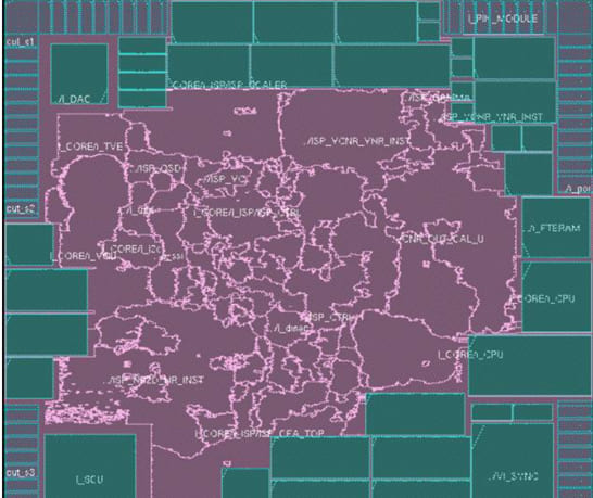
The main part of the chip area covered is divided into three parts
IO: the chip's signal and power pads, etc.
Standard cell: realize the functional logic of the chip
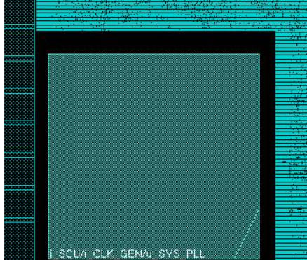
Macro block : Third party IP ( PLLDAC POR Memory .etc )
Chip area estimation is the process of counting the total area of these major parts by using the library information of the target process, the spec of the design, the information of previous designs and the comprehensive report of some IPs.
Chip area estimation
Obtaining area information
Get IO area: get the length, width and size of various IOs from the IO library file of the target process, and then count the pad selection and quantity according to the design spec, pin_list document.
Get Standard cell area: can be counted by individual IP synthesis over, conversion project section according to the original design of the full chip synthesis to get, with no complete RTL IP, according to the complexity of the IP by the design side to provide the estimated number of equivalent logic gates, through the number of equivalent logic gates * to calculate the area.
Equivalent logic gates: The complexity of the digital design is generally evaluated by the number of equivalent logic gates. Equivalent logic gates are generally a standard size (minimum drive capability) with and without gates under the target process expressed as A(10k Gates) B(um2) = C(mm2), SMIC 110nm B=4.12.
Get the Macro block area: the shape and area will be available in the IP document provided by the third-party IP provider, and the shape and area of the memory will be available in the memory document generated by Memorycompiler
Several methods of area estimation
With the above three types of area basic information, it is possible to perform area estimation.
First of all, the area information of Standard cell and Marco block should be converted. The conversion of Standard cell (if the total area of Standard cell is required to do SCAN but SCAN is not inserted, the area increment after multiplying by one SCAN is required, the empirical value is 105%) is mainly due to density, need to divide the total area of Standard cell by the density value, Macro block is mainly due to blockage, need to add the length and width of Macro block plus twice the width of blockage and then do the product.
density: Due to the chip Timing and other reasons, the area used to place the Standard cell can not be filled by the Standard cell, the total area of the Standard cell accounted for the percentage of the area used to place the Standard cell is density.
Blockage: Third-party IP (mostly analog IP) in order to prevent electrical interference from the peripheral environment, in the document will require the retention of a certain empty area or surrounded by power rings, this part of the area is blockage.
1.Pad Limit
This case is the chip all IO in the four sides of the close row full, the middle area is greater than the sum of the converted Standard cell and Macro block, because the four sides of the row full IO no way to shrink, so the main body of the chip area is the area of this area of the IO arrangement decision, do not need to estimate by the back-end engineers to arrange the IO directly given
2. Core Limit
This case is the chip all IO in the four sides of the tightly lined up, the middle area is less than the CORE area (the sum of the converted Standard cell and Macro block), then the area of CORE determines the size of the chip area.
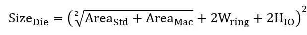
3. Core Limit, if the design has the requirement that no other cells can be placed on the IO ring, estimate the CORE as a square (because the square in the chip production in the wasted area of the wafer minimum, but also conducive to the chip internal power wiring, reduce IRdrop), the area value squared to the side length of the square plus a width of a fixed value or a percentage of the side length of the ring (power ring, etc.) twice the width, plus twice the height of the IO, and then squared to get the body of the chip area.
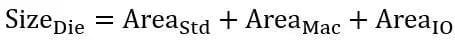
If the design of Core Limit does not require other units to be placed on the IO ring, the estimate is to add the CORE area to the IO area.
When the chip is produced many chips on a wafer need to use the scribing machine to split the chip, this time it is necessary to divide the space reserved for the chipscribe line, in the process of splitting the chip and chip transport packaging, the stress of the chip edge will change, the design needs to do a circle around the chip passivation area (sealring) to protect the chip does not The design requires a passivation area (sealring) around the chip to protect the chip from breaking as well as shielding and moisture-proof function.
The area of the chip is the length of the chip body (square of the body area) plus twice the width of the scribe line and twice the width of the sealring squared.

IO, Standard cell,Macroblock
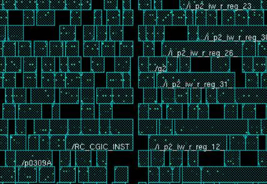
Standard cell, unused area (includes power wiring)


-20x20-20x20.png)

