IC Packaging Technology
Brief Overview
IC packaging is the circuit pins on a silicon wafer that are connected to an external connector with wires for connection to other devices. The package form is the housing used to mount the semiconductor IC chip. It has the function of mounting, fixing, sealing, protecting the chip, and enhancing the electrical and thermal performance.
Advanced IC packaging is a major technology highlight of the "More than Moore" era. When the chip in each node of the chip scaling becomes more difficult and expensive, engineers will put multiple chips into advanced packaging, and no longer have to struggle to shrink the chip.
This article provides a brief overview of the 10 most common terms used in next-generation IC packaging technologies.
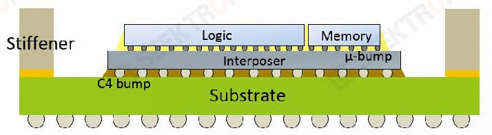
2.5D Packaging
2.5D packaging is an advancement of traditional 2D IC packaging technology that allows for finer line and space utilization. In a 2.5D package, the die is stacked or placed side-by-side on top of an intermediate layer with silicon via vias (TSVs). The base, or intermediary layer, provides interconnection between the chips.
The 2.5D package is typically used for high-end ASICs, FPGAs, GPUs and memory cubes. 2008 saw Xilinx divide its large FPGAs into four smaller chips with higher yields and connect these chips to the silicon intermediate layer. 2.5D packages were thus born and eventually became widely used for high bandwidth memory (HBM) processor integration.
3D Packaging
In a 3D IC package, logic die are stacked together or with storage die, eliminating the need to build a large system-on-chip (SoC). The die are connected to each other through an active interposer layer. 2.5D IC packages use conductive bumps or TSVs to stack components on the interposer layer, while 3D IC packages connect multi-layer silicon wafers to components using TSVs.
TSV technology is a key enabling technology in both 2.5D and 3D IC packages, and the semiconductor industry has been using HBM technology to produce DRAM chips in 3D IC packages.
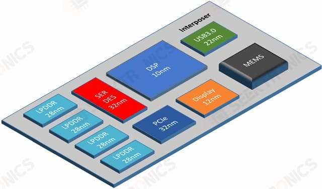
Chiplet
Chiplets are another form of 3D IC packaging that enables heterogeneous integration of CMOS devices with non-CMOS devices. In other words, they are smaller SoCs or small chips, rather than one large SoC in a package.
The idea is to break down large SoCs into smaller chips to increase yields and reduce costs. Smaller chips allow designers to leverage a variety of IPs regardless of the node or technology they are manufactured on; they can be built on a variety of materials, including silicon, glass, and laminates.
Fan out
In a fan-out package, the "connection" is fanned out from the chip surface to provide more external I/O. It uses an epoxy molding material (EMC) that is fully embedded in the die, eliminating the need for processes such as wafer bumping, fluxing, flip-chip mounting, cleaning, bottom spraying, and curing. Therefore, no intermediary layer is also required, making heterogeneous integration much easier.
Fan-out technology offers smaller packages with more I/O than other package types, and in 2016 it was the technology star when Apple was able to use TSMC's packaging technology to integrate its 16nm application processor with mobile DRAM in a single package for iPhone 7.
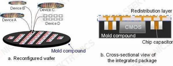
Fan-out wafer level packaging (FOWLP)
FOWLP technology is a modification of wafer-level packaging (WLP) that provides more external connections for silicon chips. It embeds the chip in an epoxy molding material, and then constructs a high-density redistribution layer (RDL) on the wafer surface and applies solder balls to form a reconfigured wafer.
Typically, it first cuts the front-end processed wafers into individual die, then separates the die on a carrier structure and fills the gaps to form the reconfigured wafer.FOWLP provides more connectivity between the package and the application board. In addition, the substrate is inherently larger than the die, so the die spacing is more relaxed.
Heterogeneous Integration
Integrating different components manufactured separately into higher-level assemblies can enhance functionality and improve operating characteristics, so semiconductor component manufacturers are able to combine functional components using different process flows into a single assembly.
Heterogeneous integration is similar to system level packaging (SiP), but instead of integrating multiple bare dies on a single substrate, it integrates multiple IPs in the form of Chiplets on a single substrate. The basic idea of heterogeneous integration is to combine multiple components with different functions in the same package.
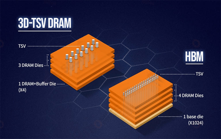
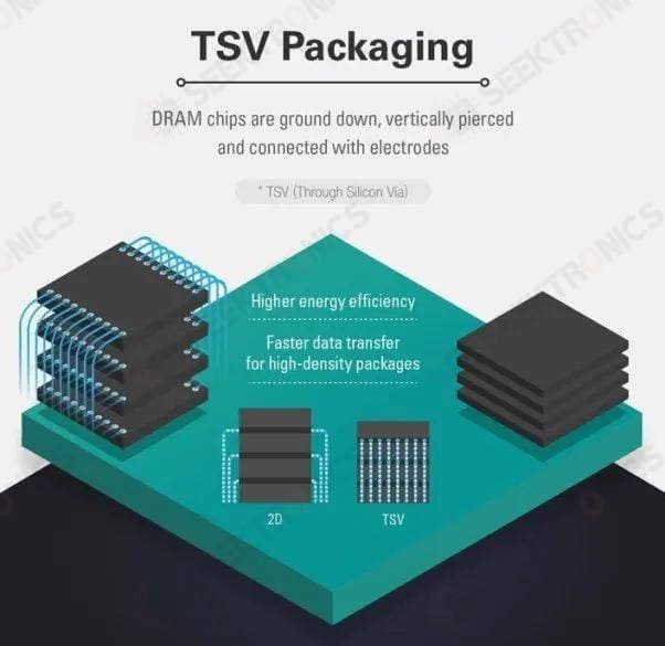
High Bandwidth Memory (HBM)
HBM is a standardized stacked storage technology that provides high bandwidth channels for data within the stack and between memory and logic components. HBM packages stack memory die and connect them together via TSV to create more I/O and bandwidth.
HBM is a JEDEC standard that vertically integrates multiple layers of DRAM components within a package, with application processors, GPUs and SoCs inside the package. HBM is primarily implemented as a 2.5D package for high-end servers and networking chips. The HBM2 release now addresses the capacity and clock rate limitations of the initial HBM release.
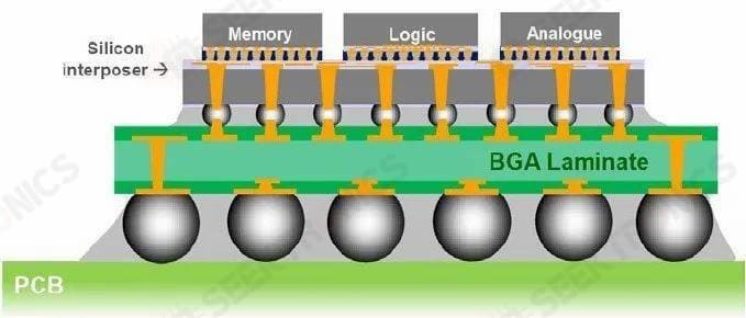
Intermediate layer
The interposer layer is the conduit through which the electrical signals are transmitted from the multi-chip die or board in the package. It is the electrical interface between the sockets or connectors, allowing the signals to travel further and to other sockets on the board.
The interposer layer can be made of silicon and organic materials and acts as a bridge between multiple die, die and board. Silicon interposer is a proven technology that plays a key role in creating 2.5D and 3D IC chip packages due to its higher fine pitch I/O density and TSV formation capability.
Redistribution Layer (RDL)
Redistribution layers are copper-metal connections or traces that electrically connect one part of a package to another. RDLs are created from layers of metal or polymeric dielectric material to stack tube cores on a package to reduce I/O spacing on large chipsets. They have become an integral part of 2.5D and 3D packaging solutions to provide communication between chips connected by intermediate layers.
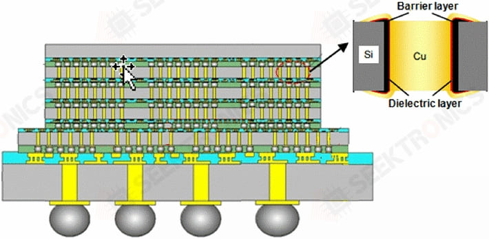
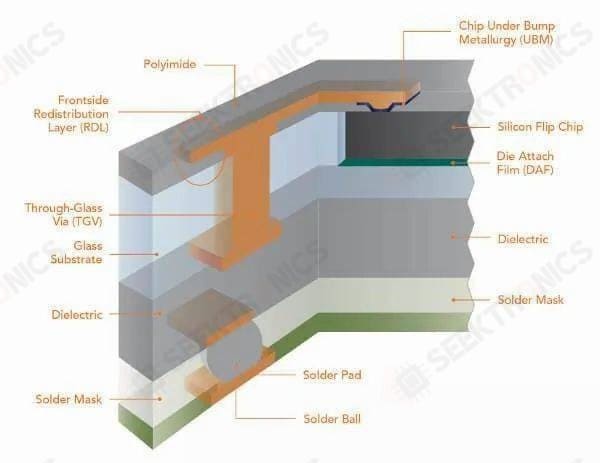
Silicon Through Vias (TSV)
TSV is a key implementation technology for 2.5D and 3D packaging solutions and is a copper-filled wafer that provides a vertical interconnect through the silicon wafer die. It runs through the entire chip to provide electrical connections, forming the shortest path from one side of the chip to the other.
The vias or holes are etched from the front side of the wafer to a certain depth, and then they are isolated and filled by depositing a conductive material, usually copper. After the chip is manufactured, the wafer is thinned from the back side to reveal the via and metal deposited on the back side of the wafer to complete the TSV interconnect.


-20x20-20x20.png)

