Many newcomers to PCBs often have this problem when they first encounter it, because the board space is too small, dense devices lead to a small space, can not lead to fan holes, usually choose to punch the holes in the pads, which makes it much easier to connect their own lines, but often do not know what kind of problems will lead to the board? Can this be done?


In order to make this issue clearly explained, it will be explained from the following two aspects:
1) Why can't via hole be in pad?
2) Under what circumstances can via holes be punched into pads?
Why can't via hole be in pad
In the early stage of PCB design, BGA pads are not allowed to have via holes. The main reason is that tin leakage leads to insufficient solder paste on the pads, which leads to virtual welding and unwelding of devices during device welding. Therefore, in general, holes are drilled on devices by leading out first and then drilling.


At present, due to the continuous narrowing of BGA spacing, tin leakage will no longer occur through the way of resin plug hole, but when the hole is hit on the pad, there will be the risk of virtual welding or falling off, which will increase the cost and affect the appearance of PCB board, so it is generally not recommended to do so.
"Monument" phenomenon often occurs in the reflow welding process of CHIP components (such as CHIP capacitance and CHIP resistance), the smaller the component volume is more likely to occur, such as 0201, 0402 and other small CHIP components. In the reflow welding process of surface mount technology, the patch element produces the phenomenon as shown in the figure. Due to the warping of one part of the component, it leads to diswelding. Because of this situation, it is generally figuratively called "monument erection" phenomenon.

The phenomenon of "monument" is due to the two ends of the component pads on the solder paste in the reflow melting, the component two solder end of the surface tension is not balanced, the tension of the larger end pulling the component along its bottom rotation and caused. Some small packages of chip resistors and capacitors, it is best not to hit the hole in the pad for the same reason, the hole in the edge of the pad, due to the tension at both ends of the pad is not the same easy to produce the monument phenomenon.

Under what circumstances can via hole be in pad
1) Buried blind hole
Generally speaking, when the pitch spacing of BGA is less than or equal to 0.5mm, BGA is not suitable for fan-out drilling. In this case, blind hole drilling can be adopted to solve the problem.
Blind vias: Blind vias are the type of holes that connect PCB inner wiring with PCB surface wiring. This hole does not penetrate the whole board. For example, only hit the top layer to the middle third layer.

Buried vias: Buried vias are the type of vias that only connect the wires between the inner layers, so they are not visible from the surface of the PCB.


Since the blind hole only goes through the surface to the inner layer, not all through PCB, so there will not be tin leakage, and the buried hole is directly drilled from the inside, so there is no such worry, the only problem is from the cost, the manufacturing cost of the buried blind hole will greatly increase.
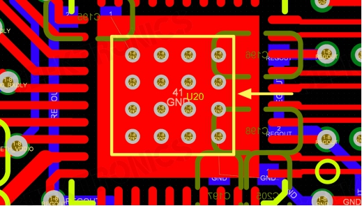
2) Heat dissipation through the hole
In PCB design, the design as shown in the figure below is often seen, which is commonly seen in the recommended design of the chip. It requires holes on the hot pad. In this case, the heat dissipation hole is played for IC heat dissipation. Because the chip body does not need to weld pins in the middle, so the hole on the IC heat sink pad is not considered tin leakage, virtual welding and other problems.


-20x20-20x20.png)

