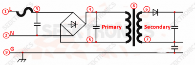
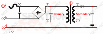
1. Transformer drawings, PCB, schematic diagrams of the three transformer fly-by-wire bit number need to be one.
Reason: Safety certification requirements
This is a fault that many engineers will make when applying for safety certification submission.
2. The discharge resistor of X capacitor should be put in two sets.
Reason: UL62368, CCC certification requires to disconnect a group of resistors and test the residual voltage of X capacitor
Many novices will make a mistake, and the only way to correct it is to change the PCB Layout again, which will waste our time and the procurement of samples.
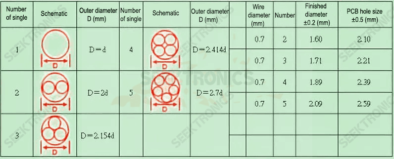
3. The PCB aperture of transformer flyline shall take into account the maximum flyline diameter. If necessary, two groups of large and small PCB holes shall be reserved.
Reason: to avoid assembly difficulties or furnace empty welding problems
Because safety application certification usually has a series, such as 24W application for a series, which contains 4.2V-36V voltage section, the output low voltage 4.2V large current and high voltage 36V small current flywire diameter is not the same.
The diameter of multiple flying wires can be calculated in the following table:
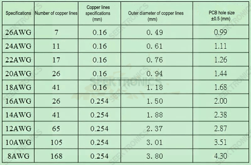
4. PCB aperture of output DC wire shall take into account the maximum wire diameter.
Reason: to avoid assembly difficulties
Because your PCB may be used for different current segments, such as 5V/8A and 20V/2A, the wire used for both will be different.
Refer to the following table:
5. Circuit debugging, multiple parallel resistance values of OCP current limiting resistors should be designed to be the same.
Reason: the higher the resistance value, the more power the resistor will bear
6. Circuit design, the holes for the heatsink pins are made into rectangular ovals (empirical value: 2*1mm).
Reason: to avoid assembly difficulties
The oval shape of the holes facilitates a space for the heatsink to move around, which is very beneficial for assembly and overheating.
7. For circuit debugging and abnormal test, the output voltage or OVP design should be less than 60VAC (VPK)/ 42.4VDC (VRMS).
Reason: Safety requirements
This novice is easier to ignore, so the product that applies for certification must do OVP test, grasp output instantaneous waveform.
8. Circuit design with electrolytic capacitors with explosion-proof holes at a distance greater than 2mm and horizontal bent feet left at 1.5mm.
Reason: Quality improvement
Generally, regular companies have this requirement, the explosion-proof holes are more important in Japan, except for special cases.
9. Emi rectification case of a 36W adapter, output 12V/3A, multi-figure comparison, and the rectification took 3 weeks.
Transformer winding method 1: NP1 →VCC→ NS1 → NS2 → copper shield 0.9TS → NP2
PCB key layout: Y capacitive ground → large capacitive ground, transformer ground → VCC capacitor → large capacitive ground
Note: All outgoes of the transformer are not crossed
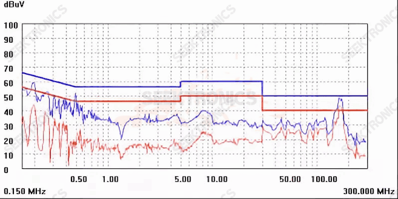
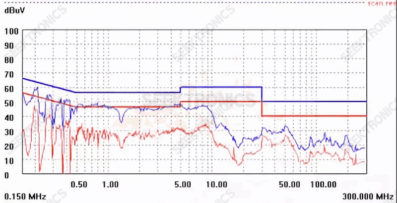
Figure 1 (115Vac)
As shown in Figure 1, the situation at 130-200m is not optimistic;
The main reason for 130-200m is the layout of PCB and Schottky circuit on the secondary side. There is little effect in other places. The magnetic beads of the Schottky set can be completely pressed down, so I forgot to save the picture.
In order to save the cost, the company did not allow me to do this, because the magnetic beads affected the cost, so I immediately removed the PCB layout and adopted the PCB key layout routing in Figure 1 A.
Transformer winding is unchanged: NP1 →VCC→ NS1 → NS2 → copper shield 0.9TS → NP2
PCB key layout: Y capacitive ground → transformer ground → large capacitor ground
Note: the primary and secondary outputs in the transformer are intersected
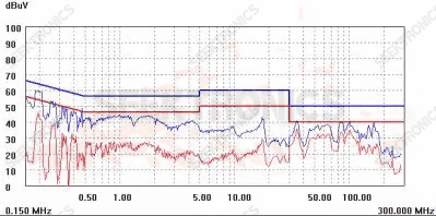
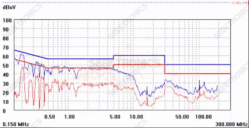
Figure 1A (115Vac)
As can be seen from Figure 1A, 130m-200m has been completely attenuated after changing the PCB layout, but the effect of 30-130m is not as good as that in Figure 1A. It may be better if there is no crossover on the transformer outgoing line. Careful observation, this IC has the function of shaking frequency, the conduction part of the frequency band cut off some spikes;
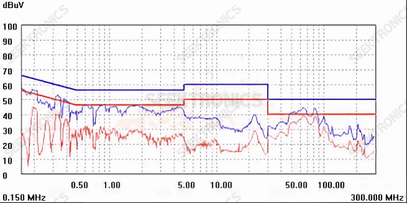
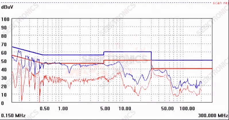
Figure IB (230Vac)
Figure IB shows that the input voltage is tested at 230Vac with a bit of top line (red line) at positions 65M and 83M
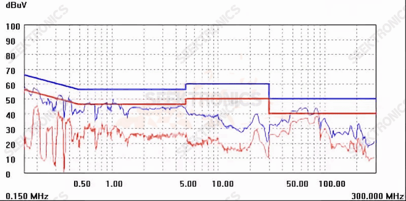
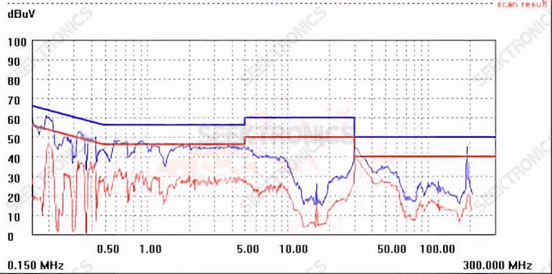
Figure 1 B-1 (230Vac)
The absorption capacitance of the primary side increases from 471P to 102P, and the position of 65M is pressed down a little, and the rear is still a little high, as shown in Figure 1B-1.
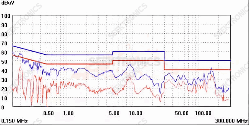
Figure IB-2 (230Vac)
Transformer shield changed to line shield (0.2*1*30Ts), fully attenuated at the back, as in Figure IB-2.
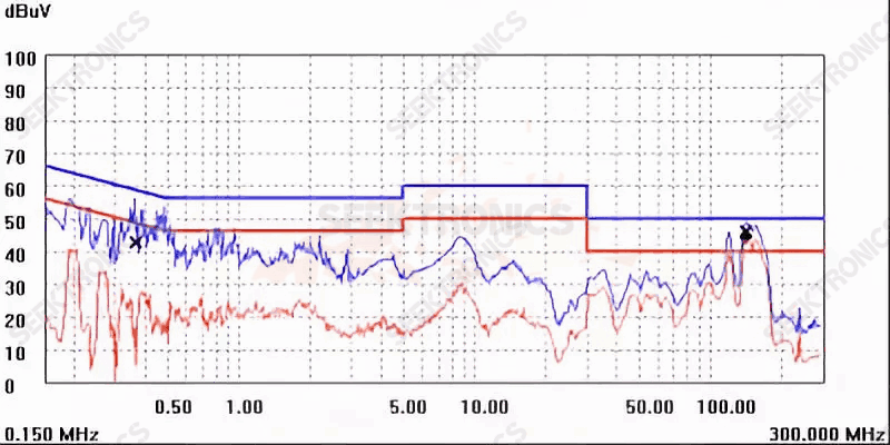
Figure IB-3 (115Vac)
115Vac input test, 150M over again at the back, fark! The high voltage is fine and the low voltage is not, annoying! Looks like this is not working.
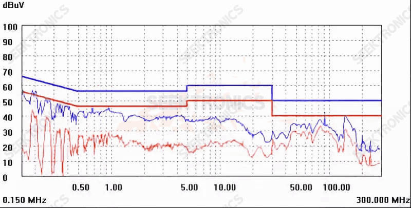
Figure IB-4 (115Vac)
The transformer shield was still replaced with a copper foil shield (the number of turns was changed from 0.9Ts to 1.3Ts), which worked well, as shown in Figure IB-4.
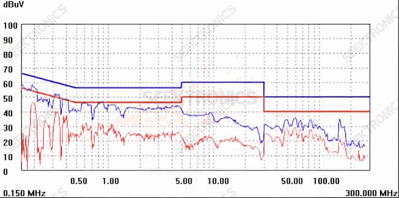
Figure IB-5 (230Vac)
115Vac input tested and passed the test.
Conclusions.
One: transformer outgoing lines need to be uncrossed.
Two: the shorter the Y-capacitor circuit alignment, the better to go through the transformer ground first and then back to the large capacitor ground, without crossing with other signal lines.
10. A 48W (36V/1.33A) rectification EMI case, just adjust the Schottky absorption will be 30-40M down.
115VAC low voltage 30M red top line
The 230VAC high pressure 30M red also tops the line
After adjusting Schottky absorption:
115VAC low pressure, very nice chart
230 VAC high voltage, very nice chart
11. List of safety distances.
12. Problems easily encountered on CAD and PADS when just starting to use.
a.. Pads drew PCB are exported as DXF files. After CAD is opened, it is a hollow line segment composed of two lines, as shown in the figure:
At first, when I didn't know how to do this, I used the L command to trace one by one, crazy.
After using it many times, the solution was to use the X command to make a single line.
b.. CAD drawing file wireframe to PADS to do PCB outer frame diagram method:
Step1. Delete no line in CAD, only the frame, other lines can also not delete.
Step2. On the keyboard, press PE, Enter, click one side of the keyboard, then press Y, Enter, Hit J, Enter, drag the mouse to select the whole frame, Enter, press ESC to exit this mode.
Step3. Scale adjustment: SC according to the space, select the entire frame, according to the space, click the mouse anywhere, scale: 39.37, according to the space.
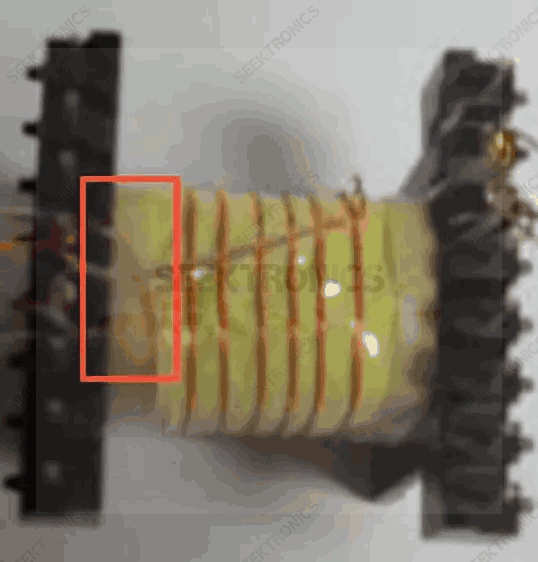
13. When drawing the PCB to define the transformer footprint, take into account whether the incoming and outgoing wires of the transformer will cross, as there is a 45-90 degree crossover between the windings at the boundary, a sleeve needs to be added to the pin at the crossed outgoing wires.
14. PCB hot spot area must be far away from the input and output terminals to prevent noise sources string to the line resulting in poor EMI, as a last resort, you can increase the ground or other shielding methods for isolation, the following figure increases a ground line for effective isolation.
Pay attention to the safety distance of this grounding line.
15. Drive resistors as close as possible to MOS, current sampling resistors as close as possible to the chip to avoid other unseen consequences.
PCB layout iron law
16. Share a radiation rectification case, a long strip heatsink has 2 feet, 2 feet are grounded, radiation hard to rectify but, later put one of the feet suspended, radiation band became good. The reason for this was that grounding the 2 feet would create a magnetic loop.
This correction cost a lot of money
17. For the power supply equipped with fan, the PCB layout should consider the wind path.
Make sure the wind gets out
18. Between the two legs of the bar inductor, remember, remember, remember, prohibit weak signal routing, otherwise you will not find the cause of the accident.
Bear in mind that we have suffered great losses on this before
19. Transformer core shape selection summary.
a. EE, EI, EF, EEL, commonly used to make small and medium power transformers, low cost, simple process
b. EFD, EPC, commonly used to produce products with height restrictions, suitable for small and medium power class
c. EER, ERL, ETD, often used to make medium and large power transformers, especially suitable for the production of multi-output high-power main transformers, and transformer leakage is small, easier to comply with safety regulations
d..PQ, EQ, LP class, the middle column of the core is larger than the general core, the product leakage inductance is smaller, suitable for small volume high-power transformers, the number of output groups can not be too much
e. RM, POT class, commonly used to make communication or small and medium power high-frequency transformers, the magnetic shielding itself is very good, easy to meet the EMC characteristics
f. EDR class, generally used in LED driver, product thickness requires thin, transformer production process is complex
20. There may be a high potential difference between certain components or wires, and the distance between them should be increased to avoid accidental short circuits induced by discharge.
For example, the distance between D and S of high-voltage MOS on the primary side of flyback is 0.85mm according to the formula 500V, and the DS voltage below 700V is 0.9mm. Considering pollution and humidity, 1.2mm is generally taken.
21. If the D-pin of THE TO220 encapsulated MOS is laced with magnetic beads, the T-pin should be considered to increase the safety distance.
I encountered the phenomenon of the exploding machine before, and it was solved after increasing the safety distance because the magnetic beads are easy to be touched with residues.
22. Send a VCC test method. Place the product in a low-temperature environment (refrigerator) for a few minutes and test whether the VCC waveform voltage triggers the chip undervoltage protection point.
Small companies don't have as much equipment, interested can do a comparison to see how different the VCC.
There are many factors to consider in the design of VCC winding number.
23. In the transformer bottom PCB with air holes, conducive to heat dissipation, the small plate is the same, to consider the wind path.
In the safety certification, the transformer temperature exceeds about 2 degrees, can use this method.
24. When there are high voltage components next to the jumper, a safe distance should be maintained, especially for components that are prone to movement or skewing.
Ensure the stability of the product during mass production
25. When the bottom of a large electrolytic output has to be jumpered, the jumper should be either low voltage or ground, with sleeves generally added to prevent the capacitor from being burned by over-wave soldering.
Avoid jumpering at the bottom of the capacitor as much as possible when designing, because it increases the cost and potential problems.
26. When the high-frequency switch tube is flat attached to THE PCB, the other side of the PCB does not put the chip and other sensitive devices.
Reason: Switching tubes work easily to interfere with the back of the chip, causing system instability, other high-frequency devices the same
27. The output DC lines should be designed to be the same length and with small pad hole spacing when the PCB is designed.
Reason: The tail length of the SR is left the same length, when the two pad holes are spaced too far apart, it will cause inconvenient production soldering
28.MOS tube and transformer are far away from AC terminal to improve EMI conduction.
Reason: The high-frequency signal is coupled out through the AC terminal, and the noise source is detected by the EMI device, causing EMI problems
29. Drive resistance should be close to the MOS tube.
Reason: Increase anti-interference ability, improve system stability
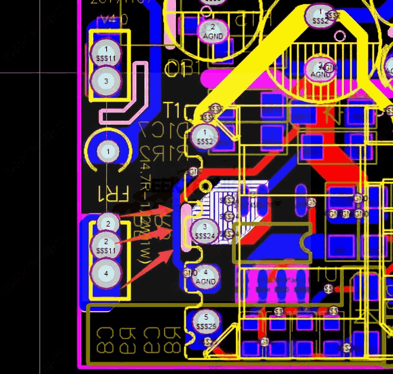
30. A PCB design routing method with constant voltage and constant current and a failure case.
For the PCB design alignment, please see the diagram at:
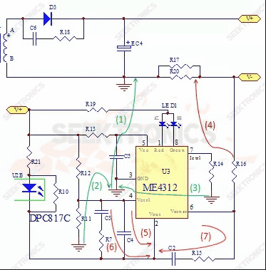
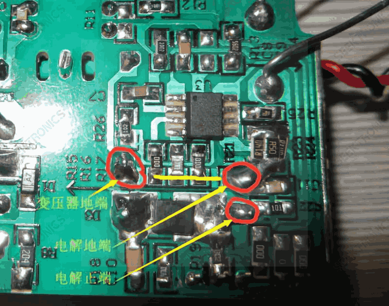
(a) The Layout principle of ground cable
As shown in the green lines (1), (2) and (3), the ground of R11 and R14 are connected to the ground of the chip, which is then connected to the ground of the EC4 electrolytic capacitor. Do not connect to the ground of the transformer, because the transformer secondary A->D3->EC4-> secondary B forms A power ring. If the ground of the ME4312 chip is connected between the secondary B line and the EC4 capacitor, strong DI/DT interference will lead to instability of the system and other factors.
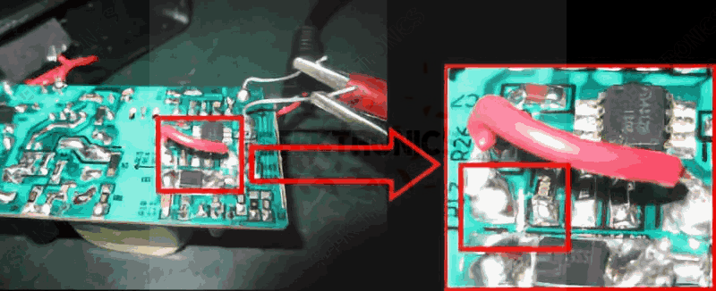
Failure cases:
Problems caused: Red and green lights come on together when the lights are turned, and red and green lights flash alternately.
Corrective measures.
By disconnecting the PCB copper foil using a wire connected to the output capacitor ground, isolating the ME4312B chip ground, as follows.
With the above treatment, the light flashing problem has been solved and the test results are as follows.
CV15V 1.043A
CV14V 1.043A
CV13V 1.043A
CV12V 1.043A
CV11V 1.043A
CV10V 1.043A
CV9V 1.043A
cv8.5v 1.043a
CV8V VCC undervoltage protection
0-94mA to green 96mA or more to red
Turning ratio 94/1043=9%, turning ratio can be controlled from 3-12%.


-20x20-20x20.png)

