Chipmakers are beginning to incorporate multiple types and flavors of DRAM in the same advanced package, setting the stage for increasingly distributed memory but significantly more complex designs.
Despite years of predictions that DRAM would be replaced by other types of memory, it remains an essential component in nearly all computing. Rather than fading away, its footprint is increasing, and so are the number of options.
There are several factors driving this expansion. Among them:
o The number and density of compute elements in a system are increasing to process more data faster, particularly for AI/ML and data center applications. More cores require more memory because there needs to be a place to store data as well as process it.
o Normally, much of this would be dealt with in cache, and SRAM has been the memory of choice for L1 through L3 cache. But SRAM no longer is scaling at the same rate as digital logic. As a result, it takes up a larger percentage of real estate on a chip, and speed improvements in DRAM have made some types suitable for L3 cache.
o Moving data back and forth is limited by bandwidth and distance, so just adding more memory in one physical location doesn’t necessarily boost performance. In fact, it may do the opposite.
For all these reasons and others, chipmakers are using more DRAM. In some cases, DRAM — particularly high-bandwidth memory (HBM) — is replacing some SRAM. DRAM has a proven track record of endurance, as well as mature processes, and it is much cheaper than SRAM. In raw numbers, SRAM may cost upwards of 2,500 times more than DRAM for the same capacity, depending on type of DRAM, according to Jim Handy, general director of Objective Analysis.[1]
There is a spectrum of DRAM available, of course. Some is very fast, such as HBM, but also expensive. Other types are slower but cheap, such as basic DDR DIMMs. What’s changed, though, is that in a heterogeneous architecture, both can play important roles, along with multiple other DRAM flavors and more narrowly targeted memories such as MRAM or ReRAM.
“We’re looking at more of a mixed model, using different DRAM technologies in the same system,” said Kos Gitchev, senior technical marketing manager at Cadence. “If you really need very high performance, and you’re willing to pay for it, then you’ll probably go for HBM. You can use that for L3 cache, or whatever else you need to access immediately. If you still need more memory, but with a little more latency, you can use DRAM in an RDIMM (registered dual in-line memory module) or an MRDIMM (multiplexer-ranked DIMM). And if you’re looking for large capacity, then maybe you’re looking at DRAM behind CXL. That technology is starting to target very specific applications with really high bandwidth and low power, larger memory footprint, but with a little more latency. Mixing all of those together is the direction everybody is going to solve those problems.”
As with nearly every improvement at advanced nodes or in advanced packaging, solving one issue can lead to another. Still, the underlying theory is sound, and there are proof points in the market today. For example, it may be essential to keep some features running at maximum speed, such as AI, which would make high-bandwidth memory the optimum choice. But not all features are essential, and they don’t all require that level of performance. In some cases, GDDR5 or GDDR6 may be sufficient. In others, it may be LPDDR, and in others maybe DDR4. There are different costs associated with all of these, and those costs can be measured in resources to move data back and forth, as well as the monetary value of the memory chips.
The flip side of this is not all DRAM is created equal, and just adding different flavors of DRAM without fully understanding how they will affect other components can cause problems. It’s important to integrate them in a way that avoids future issues, and that includes sophisticated floor planning to avoid signal integrity and prevent thermal issues. It’s well known that DRAM and heat do not go together well. But there also are a bunch of new concerns that were never seriously considered before.
“The big issues for DRAMs moving forward break down into two categories — the usual suspects (more bandwidth and capacity, managing power), and some new ones (more challenging reliability, which are causing things like on-die ECC and RowHammer protection),” said Steven Woo, fellow and distinguished inventor at Rambus. “For the new challenges, putting more capacitors on a chip is increasing the occurrence of on-die errors, so you see DRAMs today that do some amount of on-die error correction before data is returned to the controller. And neighbor cell-disturb issues like RowHammer occur because the cells are in such close proximity to each other that accessing one set of cells can cause close neighboring cells to have their bits flip.”
What works best where
The growing number of options also makes it hard to decide which memories to use. DRAM typically is chosen based on performance, power, cost, reliability (error correction code, as well as fully tested and supply-chain secure), and capacity. So if DRAM is going to be used for L3 cache, it likely will require high performance and low power. If it’s going to be used for a low-level feature in an advanced package, it may be a standard DIMM.
But each of those choices also affects the overall chip or system-in-package design and comes with specific design considerations.
“In the past, DDR4 and LPDDR4 were not over-the-top complicated,” said Graham Allan, senior manager for product marketing at Synopsys. “One customer would enable DDR4, and another would enable LPDDR4, and there was overlap. As we’ve gotten past those generations into DDR5 and LPDDR5 and beyond, those application spaces have really diverged, and so have the interface protocols and physical signaling. DDR5 typically wants to talk to tons and tons of DRAMs — large capacity — so you’re mostly interfacing to register DIMMs. With LPDDR, you’re typically talking to one package or device, and you have a maximum of two loads in that device. LPDDR is also ground-terminated. DDR is terminated to the positive voltage rails. Those are very different physical interfaces and protocols, and that means customers need to choose one or another.”
There also are some in-between options that can help utilize the same design across multiple applications. MRDIMMs, for example, either can be used to double the capacity or double the bandwidth, depending upon the workload. “Multiplexer-ranked DIMMs allow twice the capacity and a speed of up to twice that of the SDRAM (synchronous DRAM),” said Allan. “The beauty of it is the DRAMs don’t change. It operates in two different modes. It operates like a load-reduced DIMM where it doesn’t double the speed. That would be a mode where you are using it for higher capacity. Or it operates in the multiplex-ranked mode, which doubles the bandwidth between DRAMs and the external interfaces.”
That’s part of the picture. The other part is the PHY, or physical layer, which provides a physical interface to the memory. PHYs vary by the type of DRAM used, and they have become particularly important as the amount of data increases and as designs become increasingly heterogeneous.
PHYs also can be linked together into a kind of master stack in order to manage memory resources in a complex device, regardless of whether that is a GDDR6 or a LPDDR4. That way all types of DRAM can be viewed as available resources and managed centrally.
“With some type of fabric where you manage the bandwidth, everything is visible and addressable,” said Balaji Kanigicherla, corporate vice president and general manager of Renesas‘ Infrastructure Business Division. “It’s not just about improving the density, or the physics of the memory, which is material science. The application architecture of the memory is where the industry needs to go. The density needs to improve, because you want more capacity at the same bandwidth. We can mix and match based upon the path per dollar or per gigabyte, and we can use tiering between the SSD, the DRAM, and the local on-chip SRAM caches. This is shifting to a TCO for the entire system, and looking at the cost we’ll be paying for each tier.”
This essentially raises the abstraction level for memory management. “You can evolve from the current model to address memory at a global level, and basically create enough efficient interconnects to manage caching or reduce latencies,” said Kanigicherla. “It’s like a partition of global addressable memory. It’s evident that you need to provide the bandwidth. But the good news is that with AI workloads, they are a little less sensitive on latency and more sensitive to the bandwidth. So you can take this technology to scale up. Between CXL and UCIe, there should be a more gradual way to disaggregate the memory, maybe include optical interconnects, and enable a full global view of the memory. But it takes the whole industry to get there. It’s not straightforward.”
Fig. 1: Centralized control of system DRAM. Source: Renesas
Memory pooling is another option, and one that is gaining traction in data centers. Memory pooling does for DRAM what hyperscaling does for processor cores. When additional memory is needed, it is made available the same way additional compute cores are made available, usually through a CXL interface.
“The idea behind pooling is that if I’ve got a set of servers, and they’ve each got memory in them, then it’s really unlikely that each of them is using all of their memory capacity at the same time,” said Rambus’ Woo, in a recent presentation at a CASPA event. “What makes more sense is to take some of that capacity and put it in an external chassis and treat it like a pooled resource. When the processors need more than they’ve got inside the chassis, they can check out and provision some of that memory for a short period of time, use it for their computations, and then return it back into the pool. That’s one of the new features that has a lot of people in the industry excited. A little further out, once you do these types of things, you can start thinking about attaching memories and pools through switches. The CXL standard also allows for multi-level switching, as well. That kind of flexibility will help to improve both performance and total cost of ownership across a very wide range of applications.”
Other memory approaches
In addition to the more traditional approaches, DRAM is branching out in a variety of directions. In part, this is due to the shift to heterogeneous integration and advanced packaging, with more domain-specific designs, and in part because of the benefits of processing closer to the source of data.
“Comparing computation and DRAM, we are using 17% of the energy for computation and using 63% of the power moving the data from one point to the other,” said Jongsin Yun, memory technologist at Siemens Digital Industries Software. “This is a significant amount of energy. We can save that and improve speed and power efficiency. The current solution is adding more memory into cache, but that’s an expensive solution. We don’t need to move all the data to DRAM. We can do some computing in memory, or use some GPU-based AI convolution so we can do the calculation without the memory transfer.”
There are more options today than ever before, and there are many more in the development stage. Winbond, for example, developed a couple memory solutions that are based on DRAM, but which go beyond the classic DRAM use model. One is the company’s single-die CUBE (customized ultra-bandwidth element) architecture. The other is pseudo-static DRAM, which fits somewhere between SRAM and DRAM, eliminating the need for external data rewrite. Both of these are aimed at specific markets such as wearables and edge servers.
“Right now the hottest topic is generative AI,” said CS Lin, marketing executive at Winbond Electronics Corp. America. “But what’s happening in the data center has different requirements than where we are focusing, and there is very different density. We are focused on density of 16 gigabytes/second and below, but the solution is scalable down to 256 kilobytes/second. It runs at pretty close to HBM2 bandwidth, but with the advantage of very low power.”
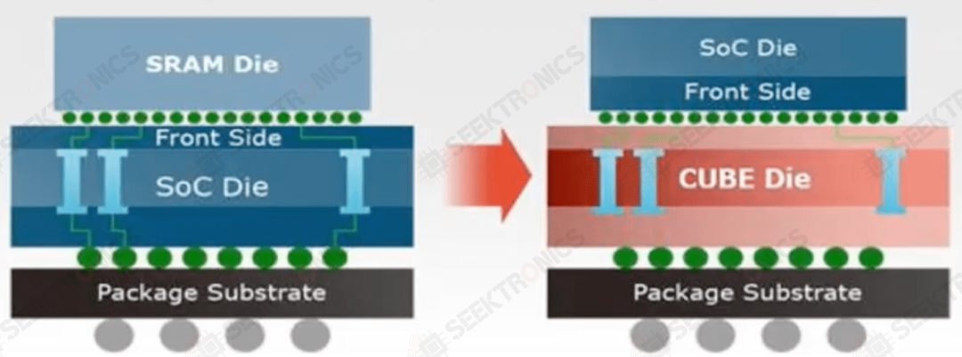
Fig. 2: CUBE approach, with ~25ns latency and 5X higher unit density than 14nm SRAM. Source: Winbond
The benefit of this approach, said Lin, is the ability to use standard DRAM to boost performance, rather than relying on the most advanced process nodes. Typically, higher density creates latency, but the CUBE architecture uses thousands of through-silicon vias to move data, with a flexible assignment of those vias based upon the need for either more bandwidth or higher speed. That allows a more granular system architecture, as well as a smaller footprint.


-20x20-20x20.png)

