In the past, analysts, consultants, and many other experts have tried to estimate the cost of new chips using the latest process technology. They concluded that by the 3-nanometer node, only a few companies could afford it, and by the E-level node, no one might be able to afford it.
Much has changed in the last few process nodes. More and more startups are succeeding in making advanced node chips that cost far less than those highly quoted numbers. Behind those numbers are some broad changes in chip design and manufacturing. Among them:
Many advanced node chips are highly replicated arrays of multiple cumulative processing elements for AI/ML. These are relatively simple compared to integrating different elements on a single chip but require characterization of their thermal issues, noise, and various use cases and applications.
Advanced packaging techniques, which have become mainstream since the creation of these early estimates, allow chipmakers to bundle together chips or chipsets developed at different process nodes, rather than trying to push analog functionality to process nodes at 5 nm or higher, which is both expensive and unproductive.
In the past, adopting the latest node ensured market leadership in terms of performance and power consumption. This is no longer the case. Improvements in mature nodes, as well as architectural changes involving hardware and software, have allowed many chipmakers to delay migration to the latest nodes, at least until these processes have matured to the point where they are cost-effective.
One of the big problems with early estimates was that they were extrapolations of the best data available at the time. The primary source of data was the International Technology Roadmap for Semiconductors, which was phased out in 2016. In the ensuing years, the fundamentals of chip design and manufacturing have changed dramatically.
For example, many assumed that all new chips would fill a reticle and that the size and complexity of designs would continue to grow. In some cases, complexity did increase - well beyond the point where all the latest features could be realized on a single reticle - but many of these new features were developed using a mix of the latest process geometries and established process nodes. In other cases, the number of process elements in the package has increased, but complexity has actually decreased.
Software is another decisive factor. Not all software needs to be developed from scratch. In addition, Arm, NVIDIA, and increasingly RISC-V designs have a large number of off-the-shelf tools and ecosystems. Almost all large EDA companies are investing heavily in AI/ML to shorten and improve the design flow, especially in software debugging and in leveraging company-wide expertise more effectively through reinforcement learning.
Some stark numbers
Back in 2018, the last time anyone made such an estimate, IBS published the chart shown in Figure 1. That chart pegged the cost of a 5nm chip at $542.2 million. If that's true, then clearly only two-thirds of the chips are in production today, and probably no one would look beyond 3nm.
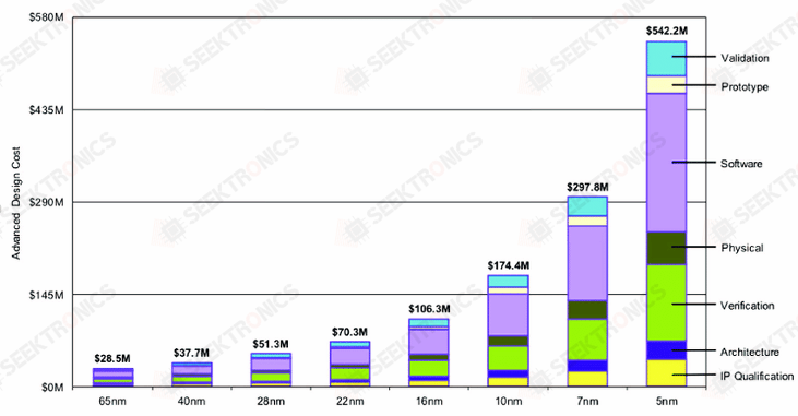
Figure 1. Cost of producing a new chip.
If we go back a few years and compare this with the chart produced by IBS in 2014 (see Figure 2), we can see how these estimates have changed over time.
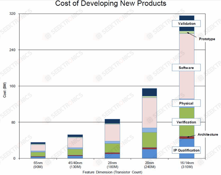
Figure 2. cost of producing new chips.
Note that the estimated cost at 16 nm/14 nm drops from about $310 million to $106 million. Going back even further, 28 nm drops from about $85 million to $51 million. Whether this is an overshoot of estimated costs or reflects a sharp drop in costs as new nodes mature is debatable. However, if the latest figures are converted to a similar amount, the cost of a 5-nanometer chip would be in the neighborhood of $280 million, and a 7-nanometer chip would cost about $160 million.
"Think Qualcomm or NVIDIA," said Isadore Katz, senior director of marketing and business development at Siemens Digital Industrial Software. If it really costs $542 million to make a new chip, only they and a few other companies can afford to do it," said Isadore Katz, senior director of marketing at Siemens Digital Industrial Software. But they're not going to make a chip at 5 nanometers. They're going to take an architecture, they're going to do some innovation on that architecture as part of the transition to the new process node, and then they're going to develop a family of parts that run on that process node.
Very few companies publish their actual costs, but you can find rough costs by looking at the venture capital the company has received to see how much they burned through when they released their first chip." "Innovium's original chip was built for $150 million, and then they raised a new round of funding for $100 million to fund multiple generations," said Nick Ilyadis, senior director of product planning at Achronix." Since its founding in 2014, Innovium has raised a total of $402 million in 10 rounds of funding and will still have $145 million in cash on hand when it sells to Broadcom in 2021 for $1 billion. Their third-generation chips are manufactured on a 7-nanometer process."
A big part of the cost is the first mover penalty." Marc Swinnen, director of product marketing at Ansys, said, "The costs associated with large digital chips have exploded." That's where those big headline numbers come from. If you look at how long it takes Apple to create a new chip, it's 18 months, hundreds of designers, licenses, a whole new set of masks and advanced processes. That's when the costs go up. But if you can use old nodes, those costs are now much lower.
There are still costs that may be hidden in these numbers." Siemens' Katz says, "Recharacterizing the functionality of the new transistors, getting mask manufacturing capabilities in place, understanding the manufacturing issues, and creating extraction models does require significant investment." However, we are leveraging lessons learned at previous nodes, and once we have completed these building blocks, BSIM-CMG models, extraction models, chip variations, and metallization, we will be able to take advantage of the upper layers of parametric or process-independent technologies."
These are the kinds of numbers that intrigue others." Frank Schirrmeister, vice president for solutions and business development at Arteris, says, "Here's a chart I drew 12 years ago (see Figure 3)." I received four or five sets of data from IBS but was unable to publish the numbers, so the chart I plotted is an average of the spending categories. This shows the main steps in chip development. It shows the timeline along the x-axis from RTL development to tape-out. It then shows the percentage of the overall project effort on the y-axis."
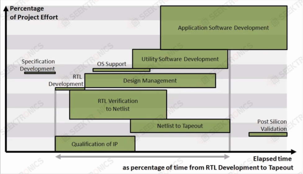
Figure 3: Time and effort required to make a chip.
Based on Figure 3, you might consider whether any of these will change over time, or with changes in size or production node. For example, it is often said that verification costs rise quadratically as chip size increases, but history has shown this not to be the case." Verification costs do go up because the larger the design, the longer it takes to simulate and the more test cases you have to generate," says Ilyadis. you can use previous generations of benchmarks and continue to run them," says Ilyadis. Then there are the new tests associated with the added features. This requires more servers, bigger servers, more disks. These all ripple through the infrastructure as additional costs.
Is the infrastructure included in the published costs?" Arteris' Schirrmeister says, "It's knowing the details of these numbers that's key." Is all the software included? How much new RTL development is included? How much verification is required? Do you need to buy emulators? When you consider the cost of the mask, that touches at least an order of magnitude of these chips."
Some of the costs do go down over time." When you consider the cost of IP, you either have to develop the IP (which requires the use of in-house engineering resources) or you have to license it (which means you pay the vendor)," says Ilyadis. Typically, licenses come with support and maintenance, which is a cash outlay," says Ilyadis. Then there's the cost of tools. Each generation requires a new set of tools as routing becomes more complex or more factors need to be taken into account. There's also the labor cost of developing the chip team. In addition, you have to build test fixtures and even products to showcase the chip. Now, we've stepped outside the realm of the chip itself, but all of this has to do with the actual development of the chip and what it takes to bring it to market. Then, there's that gift that keeps on giving - software. Most chips are programmable in some way. Beyond that, there's manufacturing, including testers, test fixtures and burn-in fixtures for accelerated life testing.
Even the cost of IP can be a significant variable, especially if one considers the time saved by purchasing the IP, or the overhead costs associated with developing it." The increased cost and complexity of SoC designs is putting more pressure on the computing infrastructure," said Brian Jeff, senior director of product management for Arm's Infrastructure business line. "This is driving the trend toward customizing silicon to provide specialized processing for specific workloads and to enable large-scale efficiency gains," said Brian Jeff, director of senior product management for Arm's Infrastructure business line. By developing IP with a customizable base, IP providers can take on many of the common integration, verification and validation tasks that partners have to repeat after design. This allows partners to focus their resources on those features that will help them differentiate themselves and design complete chips based on their workload. In one example, a partner reduced the development cost of its high-end infrastructure SoC by 80 engineering years."
Many costs are incremental." Katz says, "We don't relearn everything between process nodes." We remember what we have to do. We put a lot of effort into parameterizing or designing representations of artifacts, from the topmost testbench, to the way we describe IP, to the way we articulate custom logic and gas pedals, all the way down to how we lay out cells. We understand what needs to be tweaked and corrected with dials and knobs. You don't start from scratch between nodes. Even if we change the way a transistor surface works, or if we restructure the way the first layer of personalized metal works, we need to spend extra time characterizing it. We need to spend more time understanding how to extract that characterization, and we may need to make small but modest adjustments to our battery design to accommodate that characterization. But the basic topology is there.
EDA Costs
Each node creates new problems and challenges that often require EDA vendors to make significant investments in new tool or process creation. When new nodes emerge, many of the tools are rudimentary and the solutions are cobbled together, with no idea what techniques can be used to solve the problem.
Over time, the industry came to understand what worked and what didn't, and processes improved and eventually automated." Ansys' Swinnen says, "Many of the challenges were overcome by brute force." They utilized existing tools and enough people to make it work. This required working closely with vendors. It's not a process that the average mainstream chip designer has mastered. Over time, we learn from them and they learn from us. The tools are getting better and more automated, the rough edges have been smoothed out, and there are fewer manual steps in between. This has led to much higher productivity.
However, what works today may not work in the future." Katz says, "You have to plan for a whole range of things." I've been involved in timing, process changes and ground bounce. A lot of problems arise when you drop the voltage threshold below 1V. This was unknown when we went to 14 nm. Today, people understand that. People understand the problems that can occur in the timing or layout of a design. They understand the factors that they have to be aware of in terms of the impact of metals on latency and timing, and they are becoming more aware of some of the physical side effects, the sensitivity to glitch noise, the sensitivity to leakage. These are the stuff of playbooks. This handbook will take you through each of the difficult problems of the last 10 or 15 years. How can these problems be solved? How to automate them? Or, how can they be designed to solve these problems?
Figure 4 is another old chart worth revisiting. Andrew Kahng and Gary Smith analyzed design costs in 2001 to show how new EDA developments were affecting productivity. This analysis was published by ITRS in 2002.
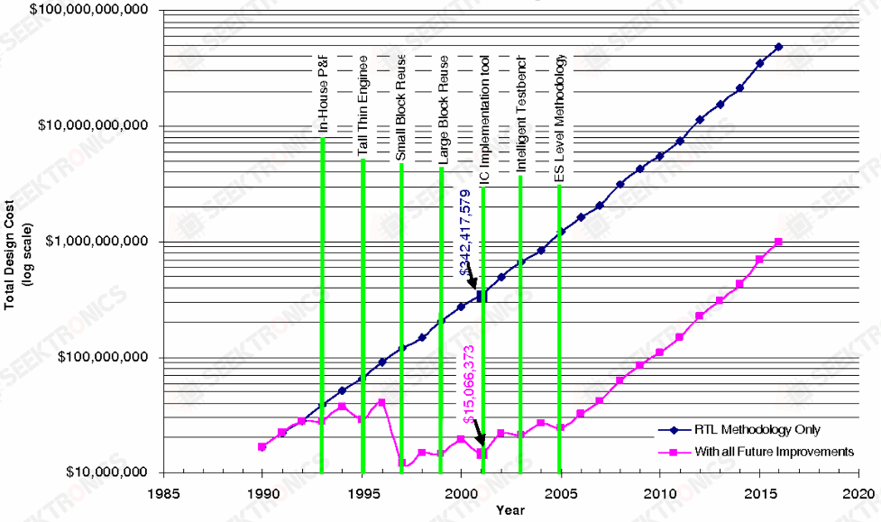
Figure 4: New Design Cost Model for ITRS 2001 Source: Proceedings of the 2002 International Symposium on High Quality Electronic Design Proceedings of the 2002 International Symposium on High Quality Electronic Design
Whilst this shows future technologies such as ESL that never existed, others did.Subsequent publications by ITRS have shown that development costs have remained somewhat stable, with only a slight increase in costs over time. Figure 5 (below) is their 2013 chart.
Figure 5: Impact of EDA on IC Design Costs, Source: Andrew Kahng, 2013: Andrew Kahng, 2013
Development costs do increase, especially for new nodes." Tools are getting more sophisticated and have to match the size of the design," Ilyadis said. "Typically, these newer tools can add up to 25% to the cost, and that's where the tool companies make their money," Ilyadis said. They have to develop, they have to work on the tools to make them compatible with the next generation of IP and to deal with any new challenges that arise, so they pass on the development costs as increased license fees.
But that's not the case with mainstream developers." The cost of EDA tools has never been a key consideration in semiconductor design economics," says Swinnen." It's a cost factor that someone has to worry about, but in the overall economics of chip design, EDA has never been the deciding factor. The determining factor is manufacturing, and the impact of EDA on design costs is more in terms of productivity.
What we are seeing is that the infrastructure costs associated with EDA tools are increasing rapidly." Schirrmeister says, "With AI being introduced into the tool suite, it's easy to start exploring the design space more." Each data point in the chart implies additional capacity and cycles to run in the cloud. To get the best implementation, you now need to spend more computational effort. What used to be people multiplied by time and some infrastructure costs now becomes a redistribution of costs, with the computational costs themselves playing a much higher role in the overall cost equation."
Conclusion
No chip has ever cost as much to develop as the published figures, for the simple reason that no chip has ever really started with a blank sheet of paper. Everything in this industry is based on the reuse of intellectual property, some of which is tied up in IP blocks, some of which is tied up in BSIM models, and some of which is tied up in the minds of the engineers who started the new company. The same is true, if not more so, of the software industry, which has always been built on a large code base.
However, all of these numbers are the right order of magnitude for cutting-edge design. It is important to understand the total cost associated with development, rather than just focusing on the production of silicon wafers


-20x20-20x20.png)

