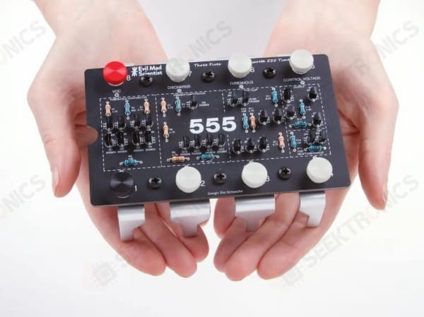
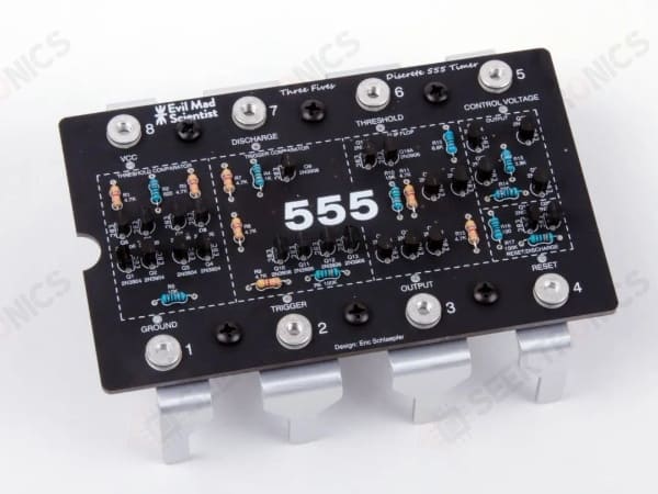
555 Timer
If you've played with electronic circuits, odds are you know about the 555 timers integrated circuit, said to be the world's best-selling integrated circuit, with billions sold. Designed by analog IC wizard Hans Camenzind, the 555 has been called one of the greatest chips of all time.
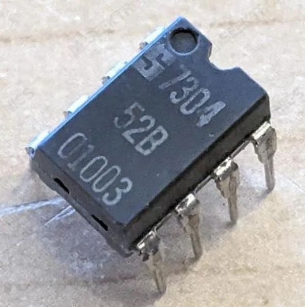
Tediously sanding the epoxy package to expose the chip (below) and identifying the chip as a 555 timer. signets released the 555 timers in mid-1972, and the chip below has a date code of January 1973 (7304), so it must be one of the earliest 555 timers. Oddly enough, it is not labeled as a 555, so it may be a prototype or internal version. I took detailed photos of the die, which are discussed in this blog post.
A brief description
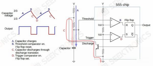
The 555 timer has hundreds of applications, from timers or latches to anything from voltage-controlled oscillator or modulator operation. The following diagram illustrates how the 555 timer works as a simple oscillator. Inside the 555 chip, three resistors form a voltage divider that generates a reference voltage for 1/3 and 2/3 of the supply voltage. An external capacitor will charge and discharge between these limits to produce the oscillation. In more detail, the capacitor will slowly charge through the external resistor (A) until its voltage reaches 2/3 reference voltage. At that point (B), the upper (threshold) comparator turns off the flip-flop and turns off the output. This turns on the discharge transistor and slowly discharges the capacitor (C). When the voltage on the capacitor reaches 1/3 of the reference voltage (D), the lower (trigger) comparator turns on, sets the trigger and the output, and the cycle repeats. The resistor and capacitor values control the time from microseconds to several hours.
In summary, the key components of the 555 timer are the comparator that detects the upper and lower voltage limits, the three-resistor divider that sets these limits, and the trigger that tracks whether the circuit is charging or discharging. the 555 timer also has two pins (reset and control voltage) that I didn't mention above, which can be used in more complex circuits.
Brief description
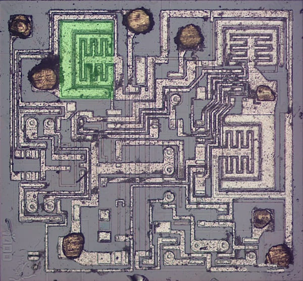
The following photo was created from a composite of microscope images. On the top of the silicon, a thin layer of metal connects different parts of the chip. This metal is clearly visible in the photograph as a light-colored trace. Below the metal, a thin layer of glassy silica provides insulation between the metal and the silicon, except for the contact holes in the silica that allow the metal to connect to the silicon. At the edge of the chip, thin wires connect the metal pads to the external pins of the chip.
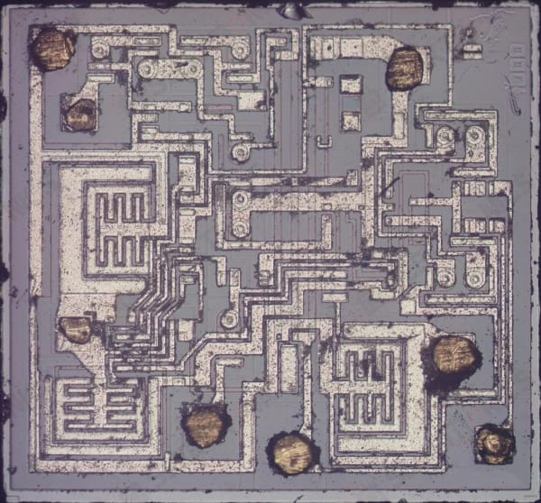
The different types of silicon on the chip are more difficult to see. Areas of the chip are treated with impurities (doping) to change the electrical properties of the silicon. n-type silicon has an excess of electrons (negative), while p-type silicon lacks electrons (positive). In the photo, these areas are shown as slightly different colors, surrounded by a thin black border. These regions are the building blocks of the chip, forming transistors and resistors. In windows, save it as a separate desktop first, then drag it in and overwrite it!
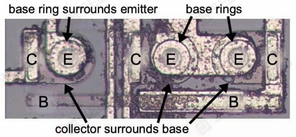
The NPN transistors inside the IC
Transistors are the key components in the chip. 555 timers use NPN and PNP bipolar transistors. If you have studied electronics, you have probably seen the NPN transistor diagram shown below, showing the collector (C), base (B), and emitter (E) of the transistor. The transistor is illustrated as P silicon sandwiched between two symmetrical N silicon layers, and the NPN layers make up the NPN transistor. As it turns out, the transistor on the chip doesn't look like this, and the base is usually not even in the middle!
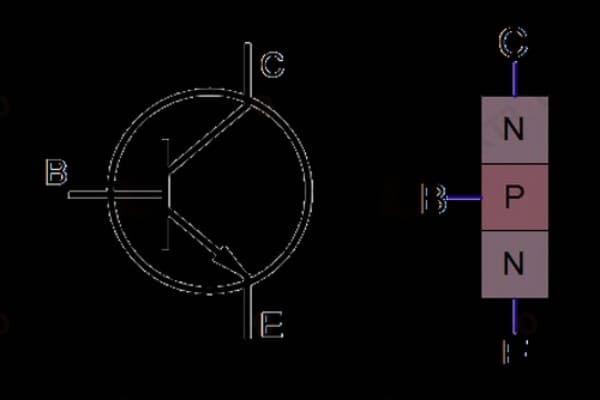
The photo below shows a close-up of one of the transistors in the 555 as it appears on the chip. The slightly different shades in the silicon indicate areas that have been doped to form N and P regions. The white areas are the metal layers of the silicon top chip - these form the wires that connect to the collector, emitter and base.
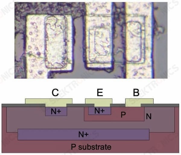
Below the photo is a cross-sectional view that illustrates the way the transistor is constructed. There is a lot more to it than the NPN you see in the book, but if you look closely at the vertical cross section below the "E" you will see the NPN that forms the transistor. the emitter (E) wire is connected to the N+ silicon. Below that is the P layer connected to the base contact (B). Below it is the N+ layer that is (indirectly) connected to the collector (C).6 The transistor is surrounded by a P+ ring that isolates it from the adjacent components.
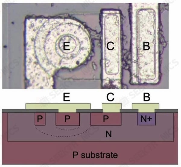
PNP transistor inside the IC
How resistors are implemented in silicon
Resistors are a key component of analog chips. Unfortunately, the resistors in ICs are large and inaccurate. Resistors can vary by as much as 50% from chip to chip. Therefore, it is important to design analog ICs with only ratios of resistors, not absolute values, because the ratios remain almost constant.
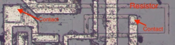
The photo above shows a 10KΩ resistor in the 555, formed by a strip of P silicon (pinkish gray) in contact with metal wires at both ends. Other metal wires run through the resistor. The resistor has a spiral shape to make its length fit into the available space. The resistor below is a 100KΩ pinch point resistor. The N silicon layer on top of the sandwich resistor makes the conductive area thinner (i.e. clips it), creating a higher but less accurate resistance.
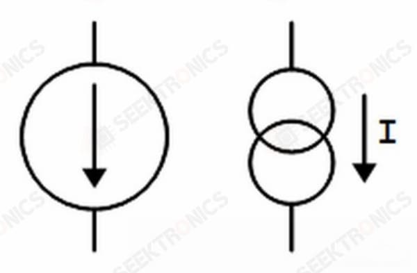
IC Components: Current Mirror
There are some subcircuits that are common in analog ICs, but may seem mysterious at first. The current mirror is one of them. If you've seen an analog IC block diagram, you've probably seen the symbols below that indicate a current source and wondered what the current source is and why it is used. The idea is that you start with a known current, and then you can "clone" multiple copies of the current with a simple transistor circuit, the current mirror.
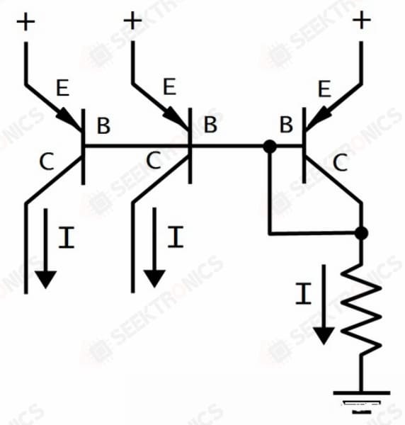
A common use of current mirrors is to replace resistors. As mentioned earlier, the resistors inside the IC are both large and inaccurate, an inconvenience. Whenever possible, space is saved by using current mirrors rather than resistors. In addition, unlike the current generated by two resistors, the current generated by a current mirror is almost identical.
IC Components: Differential Pairs
The second important circuit to understand is the differential pair, which is the most common dual-transistor subcircuit in analog ICs. You may be wondering how a comparator compares two voltages, or how an operational amplifier subtracts two voltages. This is the work of a differential pair.
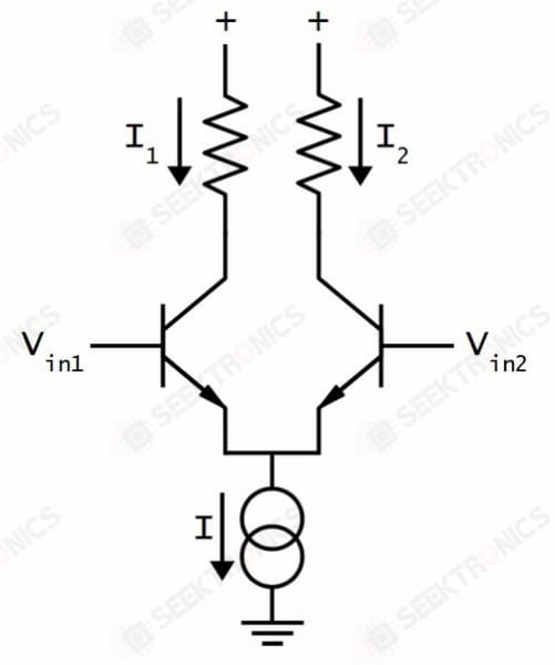
The schematic above shows a simple differential pair. The current source at the bottom provides a fixed current, I, which is divided between the two input transistors. If the input voltages are equal, the current will split equally into two branches (I1 and I2). If one of the input voltages is a little higher than the other, the corresponding transistor will conduct more current exponentially, so one branch gets more current and the other branch gets less. A small input difference is enough to direct most of the current to the "winning" branch, which turns the comparator on or off. 555 chips use one differential pair as the threshold comparator and another pair as the trigger comparator.
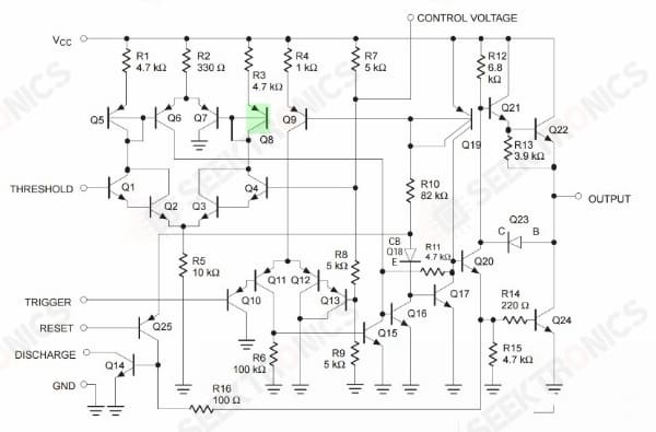
555 Schematic
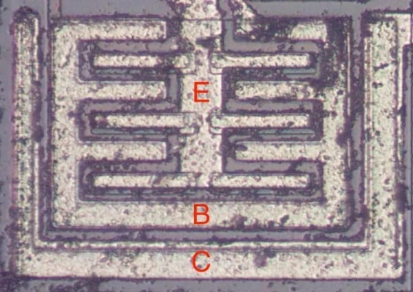
The 555 die photo and schematic below are interactive. Clicking on a component in the schematic will display a brief description of the component. For a quick overview, the large output transistor and the discharge transistor are the most obvious features on the die. The threshold comparator consists of Q1 through Q8. The trigger comparator consists of Q10 to Q13 and the current mirror Q9. Q16 and Q17 form the trigger. The three 5KΩ resistors that make up the voltage divider are located in the middle of the chip. Legend has it that the 555 is named after these three 5K resistors, but according to its designer, the 555 is just any number in the 500 chip family.


-20x20-20x20.png)

