Description of the phenomenon.
A plastic enclosure product with an I/O cable was found to exceed the radiation emission limit when conducting the radiation emission test specified in the EMC standard, specifically at 160 MHz. the cause of its radiation exceedance needs to be analyzed and appropriate countermeasures are given.
Reason Analysis
This product has only one PCB, which has a crystal with a frequency of 16MHz. It can be seen that the 160MHz radiation should be related to the crystal (Note: it does not mean that the radiation exceeds the standard is caused by the direct radiation of the crystal, may be multiplier generated). Figure 1 shows the product's local PCB layout, from Figure 1, it is clear that the 16MHz crystal is arranged right at the edge of the PCB.
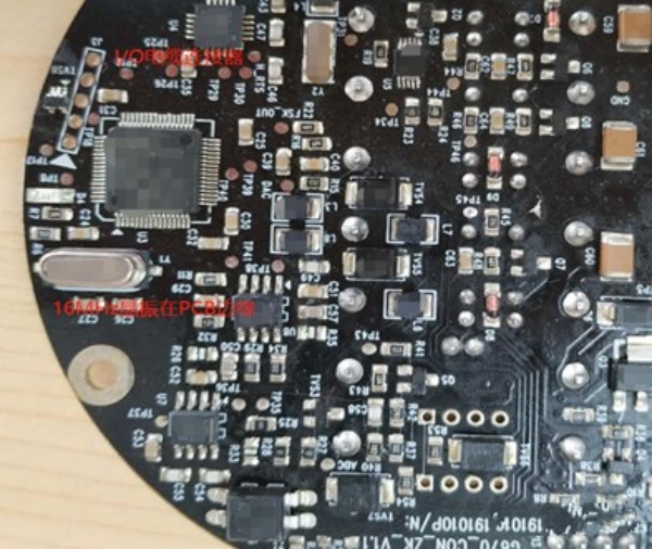
Figure 1 The product's local PCB layout of the actual diagram
In signal lines or high-speed devices and the laboratory between the reference grounding plate, there is an electric field distribution or parasitic capacitance, this parasitic capacitance is very small (such as less than 0.1pF), but will still lead to a kind of common-mode radiation in the product, the principle of generating this common mode radiation as shown in Figure 2. In Figure 2, the voltage on the crystal shell (shell not connected to the earth crystal) or the crystal clock signal pins on the voltage Udm and the reference ground between the parasitic loop, the common mode current in the loop through the cable to generate common-mode radiation, common-mode radiation current Icm ≈ C * w * Ulm, where C is the PCB signal printed line and the reference ground between the parasitic capacitance, about a tenth of a picofar to a few picofar between; Cp for the reference ground Cp is the parasitic capacitance between the reference ground and the cable, which is about 100 pF; w is the signal corner frequency. Common mode radiation current Icm will be between a few micro-amps to tens of micro-amps, the analysis shows that the common mode current flowing through the cable of this order of magnitude is sufficient to cause the radiation emission test exceeds the standard.
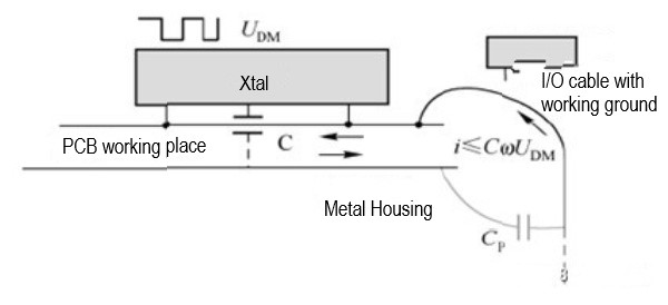
Fig. 2 Principle of radiation emission due to capacitive coupling between crystal oscillator and reference ground plate
Why the crystal arrangement in the PCB edge will lead to radiation exceeding, and to the board after moving, can make the radiation emission test pass it?
From the above analysis can already be seen, the crystal and the reference ground between the coupling of the cable common mode radiation is the essence of the crystal and the reference ground between the parasitic capacitance, that is, the larger the parasitic capacitance, the more powerful the coupling between the crystal and the reference ground, the greater the common mode current flowing through the cable, the greater the common mode radiation emission generated by the line; and vice versa, the smaller the radiation emission. What is the essence of this parasitic capacitance? In fact, the parasitic capacitance between the crystal and the reference ground is due to the electric field distribution between the crystal and the reference ground, when the voltage difference between the two is constant, the more the electric field distribution between the two, the greater the electric field strength between the two, the greater the parasitic capacitance between the two. When the crystal is arranged at the edge of the PCB, the electric field distribution between the crystal and the reference ground is shown in Figure 3. When the crystal is arranged in the middle of the PCB, or far from the edge of the PCB, the electric field distribution between the crystal and the reference ground plate is shown in Figure 4.
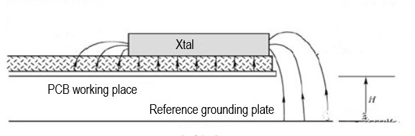
Figure 3: Electric field distribution between the crystal at the edge of the PCB and the reference ground plane
From the comparison of Figure 3 and Figure 4, we can see that when the crystal is arranged in the middle of the PCB, or far from the edge of the PCB, due to the presence of the working ground (GND) plane in the PCB, so that most of the electric field is controlled between the crystal and the working ground (GND), that is, inside the PCB, the electric field distributed to the reference ground is greatly reduced, that is, the parasitic capacitance between the crystal and the reference ground is greatly reduced. At this point it is not difficult to understand why the crystal arrangement at the edge of the PCB will lead to excessive radiation, and after moving to the inside of the board, the radiation emission is down.
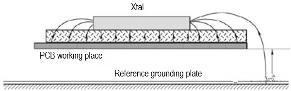
Figure 4 PCB middle of the crystal and the reference ground between the electric field distribution diagram
Treatment measures.
Option 1: Move the crystal inward so that it is at least 1 cm away from the edge of the PCB ground plane, and lay copper on the PCB surface within 1 cm from the crystal, while the copper on the surface is connected to the PCB ground plane through the vias.
Option 2: Without changing the circuit board, we choose to abandon the use of the external crystal oscillator, shield the external crystal oscillator in the software, and use the internal crystal oscillator of the microcontroller.
The experiment uses program one, after the modified test results have significantly improved, as shown in Figure 5 below, the left and right are before and after the rectification of radiation emission test spectrum before and after the rectification, it can be clearly seen after the rectification, radiation emission has significantly improved
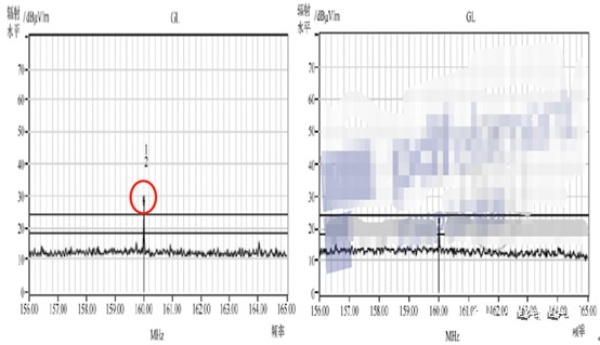
Fig. 5 The spectrum of radiation emission test before and after the correction
Reflections and Insights
(1) The capacitive coupling between printed lines or devices with high dU/dt and the reference ground plane will create EMI problems, and the placement of sensitive printed lines or devices at the edge of the PCB will create immunity problems.
(2) Eliminate high dU/dt printed lines or devices placed at the edge of the PCB, if the design must be arranged at the edge of the PCB for other reasons, then you can lay another working ground (GND) line on the edge of the crystal printed lines, and pay attention to be sure to punch a hole in the package ground line at some distance to enclose the crystal part, as shown in Figure 6 below.
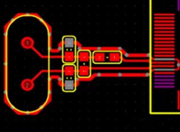
Figure 6 Schematic diagram of the crystal-wrapped ground
The theoretical basis is the same as the Faraday cage: due to the electrostatic equipotential of the metal, it can effectively shield the external electric field of electromagnetic interference. Faraday screen cage no matter how high the voltage is added inside there is no electric field. And because of the conductivity of the metal, even if the cage is through a large current, the internal objects through the current is minimal. In the face of electromagnetic waves, it can effectively prevent the entry of electromagnetic waves.
Due to the principle of electrostatic shielding of Faraday screen cages, people in cars, airplanes and other vehicles are not struck by lightning. Likewise, coaxial cables with metal sheaths can transmit signals without interference because of the Faraday shield principle. If there is no repeater in the elevator, then when the elevator is closed, any electronic signals inside can not be received. To prevent interference, some precision instruments need to be placed in the cage before operation or measurement. Or you can also open another hole, such as the metal body construction of the smartphone.
(3) to eliminate a misconception: do not think that the radiation is directly caused by the crystal, in fact, the crystal is small, it directly affects the near-field radiation (manifested by the crystal and other conductors (such as the reference ground) between the formation of parasitic capacitance), the direct factor causing far-field radiation is the largest size of the cable or product and the radiation frequency wavelength can be compared to the conductor.
(4) In addition, grounding the crystal housing can reduce this interference superimposed on the system to some extent.


-20x20-20x20.png)

