Storage and computation, or computation in storage, refers to the transformation of the traditional von Neumann architecture from a computation-centric design to a data storage-centric design, that is, the use of memory for data computation, thus avoiding the "storage wall" and "power wall" generated by data handling This avoids the "storage wall" and "power wall" generated by data handling, and greatly improves the parallelism and energy efficiency of data. This architecture is especially suitable for end devices requiring large computing power and low power consumption, such as wearable devices, mobile devices, smart homes, etc.
1. Limitations of the von Neumann architecture
The first is performance.
In the classical von Neumann architecture, data storage and computation are separated, and data is exchanged between processor CPU memory through the data bus. However, due to the different internal structures, processes, and packaging of processors and memories, the performance of the two also differs greatly. Since 1980, the performance gap between the processor and the memory has been widening, the memory access speed is far from the CPU data processing speed, which travels between the memory and the processor a "storage wall", which seriously restricts the overall performance of the chip.
The second is power consumption.
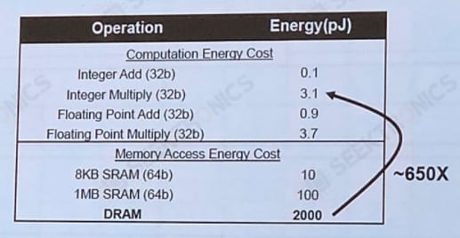
As mentioned earlier, due to the separation of processor and memory, in the process of processing data, the data first needs to be carried from the memory to the processor through the bus, and after the processing is completed, the data is carried back to the memory for storage. The energy consumption during data handling is 4 to 1000 times higher than that of floating-point operations. With the advancement of the semiconductor process, although the overall power consumption decreases, the power consumption ratio accounted for by data handling is getting larger and larger. According to the study, in the 7nm era, the sum of access memory power consumption and communication power consumption occupies more than 63% of the total power consumption of the chip.
Due to the existence of the above storage wall and power wall bottlenecks, the traditional von Neumann architecture is no longer suitable for AIoT scenarios that focus on big data computing, and the need for new computing architectures has arisen.
2. Solution ideas
For the design of new computing architectures, researchers have proposed a variety of solutions, which are broadly classified into three categories.
(1) High-speed bandwidth data communication, including optical interconnection and 2D/3D stacking.
High-speed bandwidth data communication alleviates the storage wall problem mainly by increasing the communication bandwidth. Optical interconnect technology enables high-speed data transmission and reduces power consumption. 2.5D/3D stacking technology is to stack multiple chips together to enhance communication bandwidth by increasing the parallel width or using the serial transmission.
(2) Near-storage computing.
The basic approach of near-storage computing is to store data as close as possible to the computing unit, thus reducing the latency and power consumption of data handling. Currently, the architecture of near-storage computing mainly includes multi-level cache architecture and high-density on-chip storage.
(3) Storage computing in one, i.e., the algorithmic embedding of the memory itself.
The core idea of storage computing or in-store computing is that by embedding algorithms in the memory cell itself, computing can be done within the memory cell.
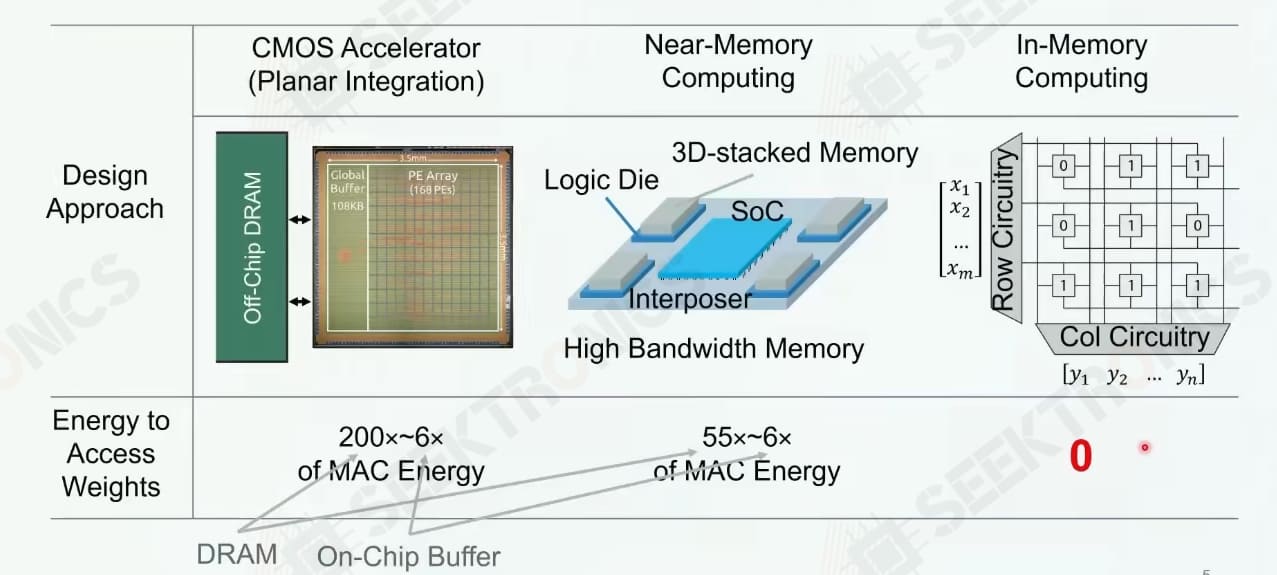
Power Consumption Comparison
A comparison of the power consumption of traditional off-chip storage, near-storage computing, and in-storage computing can be found in the following figure.
3. Memory-computing chip features
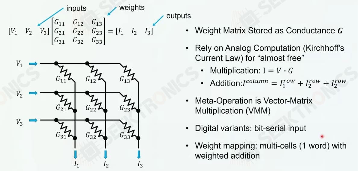
As we mentioned earlier, the core idea of memory-computing integration is to embed the algorithm in the memory unit itself, specifically, the weight data of the AI model is stored in the memory unit, and then the core circuit of memory is designed so that the process of data flow is the process of the dot product of input data and weight in the analog domain, which is equivalent to the accumulation of input with weight, that is, convolutional operation. Since the convolutional operation is the core component of the deep learning algorithms, the integrated storage and computation are well suited for deep learning. The architecture completely eliminates access latency and greatly reduces power consumption, which is a true convergence of storage and computation. At the same time, because computation is fully coupled to storage, finer-grained parallelism can be developed for higher performance and energy efficiency.
4. Status of the integrated storage and computing chip
(1) Technology implementation method
According to the classification of volatility during the storage period, the implementation of the storage and computing technology can be roughly divided into two ways.
volatile-based, existing process mature SRAM, DRAM implementation.
Implementation based on non-volatile, new memories such as phase change memory PCM, resistive memory RRAM/reminder ReRAM, floating gate devices or flash memory Flash.
Volatile memory SRAM and DRAM are mature processes and are the main memory products commercially available today. Therefore, many vendors and research institutes have started to conduct research on in-store computing based on SRAM and DRAM. However, due to the different manufacturing processes of current memories and processors, a good balance between processing performance and storage capacity cannot be achieved yet.
Non-volatile memories include spin moment magnetic memory STTRAM, phase change memory PCM, resistive memory RRAM, etc. These memories have been developed rapidly in the last decade or so, and their capacity has been increasing, and they have a natural integration of computation and storage. However, due to the immaturity of the corresponding vendors and processes, there is still a certain distance from real commercialization.
(2) Competitive landscape
In recent years, a number of domestic and international DIC startups have emerged.
Some of the more famous foreign DIC startups include Mythic and Syntiant, while the old giant Samsung has also developed its DIC technology based on HBM2 DRAM.
Domestic companies are even more blossoming, including ZhiCun Technology (based on Flash), Flash Billion Semiconductor (based on memory resistor PLRAM), XinYi Technology (based on RRAM), HengShuo Semiconductor (based on NOR Flash), HouMo Intelligent (research direction including SRAM/MRAM/RRAM), JiuTianRexin (based on SRAM), etc. In addition, there is Ali Pinto (3D bonding stack based on DRAM).


-20x20-20x20.png)

