31. A recent chip capacitor price coping tips, chip capacitors are reserved for a plug-in position, or 104 are changed to 224P, which is relatively cheaper.
32. Circuit debugging, output circuit with LC filter needs to be aged to confirm the ripple, if the ripple is abnormal please adjust the loop.
Reason: verify the stability of the product
This is very important, I often encountered this problem before, the production line after aging test ripple will become high, the phenomenon is the loop oscillation.
33. Circuit debugging. When the diodes are connected in parallel, it is necessary TO test the abnormality caused by the fault opening of one diode (including the two diodes in TO-220).
Reason: Quality improvement
Small companies generally do not do this action, a good product is to withstand any test.
34. Circuit design, if PCB space is sufficient, please design to pass all safety standards.
Reason: Reduce the number of PCB modifications.
If one of your products meets the UL60335 standard and the customer wants to meet THE UL1310 one day, then you have to change the PCB Layout and report it to the safety regulation. If the board you draw meets all kinds of standards, the rest work will be much easier.
35. Circuit design, regarding ESD please design to contact ±8KV/air ±15KV standard.
Reason: to reduce the number of subsequent rectifications.
Customers like Philips require very strict ESD, I heard that Foxconn also needs to reach ±20KV, one day there are such customer requirements, you have to be busy again for a while.
36. Circuit design, design the transformer, VCC voltage at light load voltage should be greater than the IC's undervoltage shutdown voltage value.
Judgment of no-load VCC voltage needs to be greater than the chip off voltage of about 5V, while confirming that the full load can not be greater than the chip overvoltage protection value.
37. Circuit design, the design of common transformer should take into account the VCC voltage when the maximum output voltage is used. At low temperatures, VCC will touch OVP with a little NOSIE.
If your 9V-15V products share the same transformer, please confirm the VCC voltage and the power tube voltage.
38. circuit debugging, Rcs and Ccs values should not be too large, otherwise it will cause the VDS to exceed the maximum withstand voltage blow up.
If the LEB front fading time is set short, it will be shorter than the time of the spike pulse, which will have no effect or will be misjudged; if it is set long, the real overcurrent will not play a protective role.
Rcs and Ccs RC value must not exceed 1NS Delay, otherwise the output short-circuits, Vds will be higher than at full load, more than the maximum withstand voltage MOSFET may cause a blowout.
The empirical value of 1nS Delay is approximately equal to 1K to 100PF, also equal to 100R to 102PF
39. When drawing the small board, add a round drill hole at the 90-degree corner of the pin of the small board.
Reason: Easy to assemble
As shown in the figure:

The actual board is shown in the picture:
The actual assembly is shown in the figure:
This allows for a tight fit between the small board and the large PCB without any floating heights
40. Circuit design, the heat sink of Schottky can be connected to the output positive circuit, so that the iron sealed Schottky does not need insulation pad and insulation particles.
41. Circuit debugging, DO not use 1N4007 for RCD absorption of power above 15W, because THE speed of 1N4007 is 300uS slower, the pressure drop is also 1.3V larger, and the temperature is very high in the aging process, which is easy to fail caused by frying machine.
42. Circuit debugging, the output filter capacitor withstand voltage at least need to meet 1.2 times the margin, to avoid the phenomenon of damage in mass production.
This is a very low-level mistake, 14.5V output capacitor with 16V withstand voltage, mass production has 1% of the capacitor failure bad.
43. Circuit design, large capacitance or other capacitors made of horizontal, at the bottom of the jumper should be placed in the negative potential, so that the jumper can not wear casing.
This will save costs.
44. Rectifier bridge stack, diode or Schottky, crystal size element recognition or description in BOM, e.g. 67mil.
Reason: Control supplier delivery consistency, to avoid suppliers cutting corners and affecting product efficiency
Troublesome is the supplier to do tampering, resulting in a whole batch of trial production products can not pass the six levels of energy efficiency, the reason is the Schottky internal wafer with a small lead.
45. Circuit design, Snubber capacitors, preferred Mylar capacitors due to noise problems.
One of the ways to deal with different sounds.
46. The noise generated by the immersed TDK RF inductor is 12dB less than that of the unimmersed drum-shaped differential mode inductor and the immersed magnetic core.
The second way to deal with different sounds
47. The transformer is manufactured with vacuum dipping paint, which allows it to operate at a lower flux density, using epoxy resin vinyl to fill the gaps in the three center columns.
The third way to deal with different sounds.
48. Circuit design, start resistor if used in the rectifier before, to add a string of several hundred K resistors.
Reason: resistor short circuit, will not cause IC and MOSFET damage.
49. Circuit design, high voltage capacitor with a 103P chip capacitor position.
Reason: it has certain effect on radiation of 30-60mhz.
If space permits, please leave a place for PCB Layout, so as to facilitate EMI's rectification.
50. During EMS project testing, the maximum program of the product should be tested until the product is damaged.
For example, ESD lightning strike, etc., must hit until the product is damaged, and do a good job of relevant records, see how much product margin, do know.
51. Circuit design, abnormal test, short circuit open circuit a component if there is still output voltage then to carry out LPS test, overcurrent point can not exceed 8A.
More than 8A is not eligible for LPS.
52. Safety regulation open-shell prototype, all optional plug-in components to be installed for photography, L, N and DC lines and PCB point white glue fixed.
This is a common problem, often vigorously sent samples to third party institutions, and then back and forth to change.
53. Circuit debugging, cold PSR need 1.15 times the current to be able to boot, SSR needs 1.3 times the current to be able to boot, to avoid poor start after aging.
PSR now many chips can achieve "zero recovery" OCP current, such as ME8327N, with "zero recovery" OCP current function.
54. For circuit design, please note that the total capacity of the Y-capacitor used should not exceed 222P, because of the influence of leakage current.
The leakage current requirement is different for different safety standards and should be taken into account when designing.
55. For flyback topology structure, the value of transformer B should be less than 3500 Gauss. If the transformer is saturated, all actions will be out of control, as follows:
The magnetic saturation of the transformer must be confirmed, heavyweight, this is the first safety performance guarantee, including the magnetic saturation of the current point, the magnetic saturation of the boot moment, the magnetic saturation of the output short circuit, the magnetic saturation at high temperature, the magnetic saturation at high and low voltage.
56. For structural design, the heat sink is fixed with screws, refer to the following table for design. In practical application, the allowance of 0.5-1mm should be increased, refer to the following table:
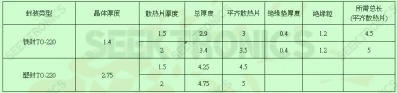
The screw specification written on BOM must be correct, otherwise it will make you uncomfortable in mass production.
57. Structure design, AC PIN solder wire needs to be hooked up, if not then white glue should be used to fix it.
Reason: Safety requirements
Samples are often returned by third-party organizations for rectification.
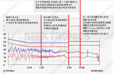
58. Conduction rectification, segmented processing experience, as shown below, is only one way of processing, and some situations are not directly applicable.
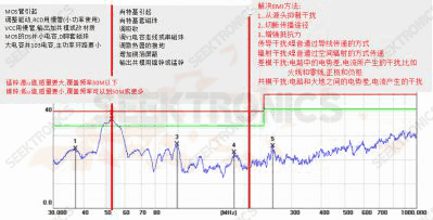
59. Radiation rectification, section processing experience, the following chart, suitable for some novice engineers, to provide a reference direction, some cases are not directly applicable, the main thing is to figure out the mechanism of EMI generation.
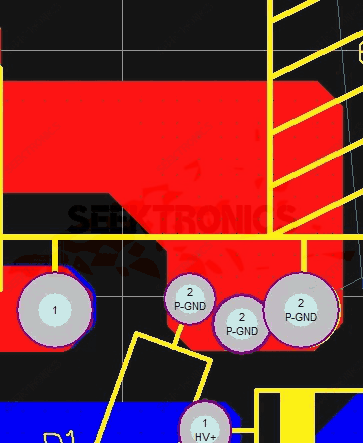
60. As for the problems encountered by PCB, as shown in the figure, why can't this position be filled when the 99SE drawing board is covered with copper? It looks like dead copper.
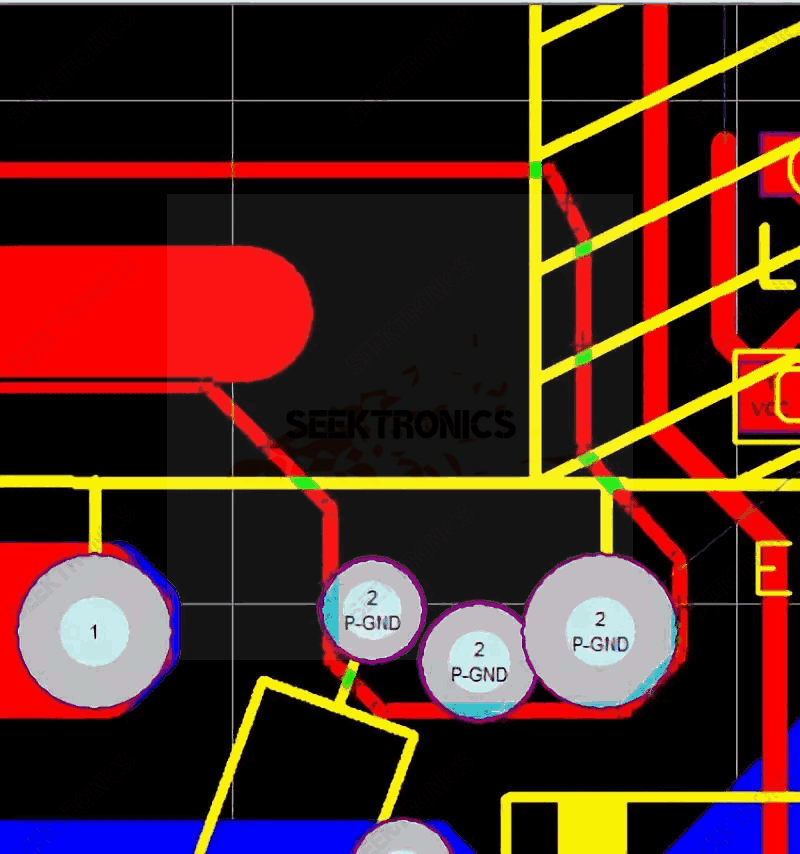
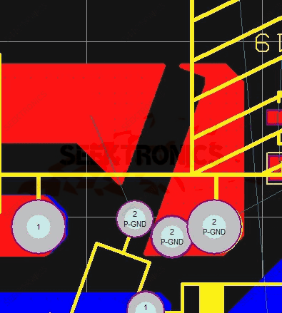
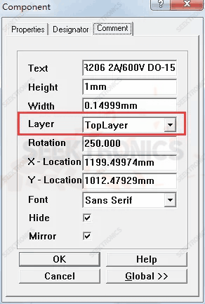
The D1 component has a text description property placed on top of the copper foil, as shown
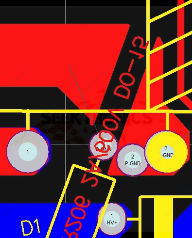
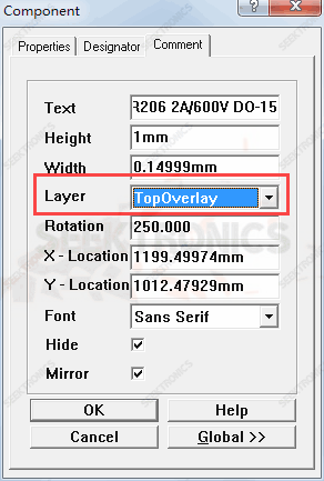
Perfect solution after putting it on the top screen print
61. Transformer copper foil shielding mainly for conduction, line shielding mainly for radiation, when the conduction is very good, it is possible that your radiation will be poor, this time to change the transformer copper foil shielding to line shielding, try to depress the position of 30M down, so that the rectification of radiation will be much faster.
EMI rectification tips No. 1
62. When testing radiation, bring more MOS and Schottky of different brands. Sometimes only 2 or 3dB difference when changing a different brand will have a surprise.
EMI rectification tips No. 2
63. The rectifier diode on the VCC, which also has a great impact on radiation.
In a painful case, a product over the EMI, the residual are more than 4dB, mass production many times, one of the mass production samplings EMI found that the radiation over 1dB or so, the defect rate of 50%, after layers of investigation, one component to replace. Eventually found that the rectifier diode on the VCC caused the problem, replace the previous tube (leave a low sample), the residual has 4dB. analysis of the bad tube found that the internal supplier of the tube to do a mirror image processing.
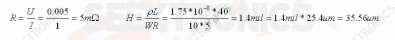
64. How to measure the copper foil thickness of PCB?
Method: Find a smooth and long line on the PCB board, measure its length L, and then measure its width W, and then measure the voltage drop U at both ends with A DC source and 1A current.
According to the resistivity formula, the following formula is obtained:
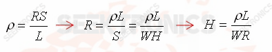
For example: take a section of PCB copper foil, the length L is 40mm, the width is 10mm, the voltage drop at both ends of the 1A current is 0.005V, how many um is the thickness of this section of copper foil?


-20x20-20x20.png)

